Silicon, the best-known semiconductor, is ubiquitous in electronic devices including cellphones, laptops and the electronics in cars. Now, researchers at the National Institute of Standards and Technology (NIST) have made the most sensitive measurements to date of how quickly electric charge moves in silicon, a gauge of its performance as a semiconductor.
Semiconductors
Cold Sintering Produces Capacitor Material at Record Low Temperatures
Barium titanate is an important electroceramic material used in trillions of capacitors each year and found in most electronics. Penn State researchers have produced the material at record low temperatures, and the discovery could lead to more energy efficient manufacturing. A team of Penn State scientists used the cold sintering process to densify barium titanate ceramics at less than 572 degrees Fahrenheit (300 degrees Celsius), the lowest processing temperatures ever used, while maintaining the quality achieved at higher temperatures in modern commercial manufacturing, the researchers said.
Micron Partners With Seven Industrial Companies to Deliver Robust and Innovative Solutions
Backed by Micron and other founding members such as Advantech, ATP Electronics, Greenliant, Innodisk, Kontron, Mercury Systems and Viking Technology, Micron’s IQ Partner Program promotes design solutions that deliver high-quality, robust and long-lasting products across a breadth of industrial applications such as factory automation, transportation and defense systems.
KLA Introduces New IC Metrology Systems
Today KLA Corporation (NASDAQ: KLAC) announced the Archer™ 750 imaging-based overlay metrology system and the SpectraShape™ 11k optical critical dimension (“CD”) metrology system for integrated circuit (“IC” or “chip”) manufacturing. As each layer in a chip is constructed, the Archer 750 helps verify that pattern features are correctly aligned to features on previous layers, while the SpectraShape 11k monitors the shapes of three-dimensional structures, such as transistors and memory cells, to ensure they remain in spec.
Winfried Kaiser Honored with the SPIE Frits Zernike Award for Microlithography
Winfried Kaiser, head of Product Strategy of ZEISS Semiconductor Manufacturing Technology (SMT) and, as the highest point of his professional career Fellow of the company, has been honored with the 2020 Frits Zernike Award for Microlithography of the International Society for Optics and Photonics (SPIE). Kaiser received the prize during the SPIE Advanced Lithography Conference in San José, California. The award is considered to be the highest honor in microlithography.
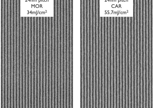
Imec Demonstrates 24nm Pitch Lines With Single Exposure EUV Lithography on ASML’s NXE:3400B Scanner
This week, at the SPIE Advanced Lithography Conference, imec and ASML announce a breakthrough in printing narrow 24 nanometer (nm) pitch lines, corresponding to the dimensions of critical back-end-of-line metal layers of a 3 nm technology node process.
D2S Extends GPU-Accelerated Wafer Plane Analysis to EUV Photomasks
D2S, a supplier of GPU-accelerated solutions for semiconductor manufacturing, today announced that its TrueMask® WPA (Wafer Plane Analysis) solution — a GPU-accelerated aerial simulation tool that integrates with mask CD-SEM systems to provide fast, highly accurate and highly repeatable CD metrology for complex and curvilinear mask shapes — has been extended for use with EUV photomasks.
Micron joins eBeam Initiative
The eBeam Initiative, a forum dedicated to the education and promotion of new semiconductor manufacturing approaches based on electron beam (eBeam) technologies, today announced that Micron has joined the eBeam Initiative. As an industry leader in memory and storage solutions, Micron will provide a unique and important perspective to the educational activities of the eBeam Initiative within the semiconductor photomask and lithography supply chain.
Advanced Semiconductor Manufacturing Strategies in AI Era to Highlight ASMC 2020
Covering topics from yield management to metrology in the era of artificial intelligence (AI), more than 100 industry experts will deliver 35 hours of technical presentations on the latest advanced semiconductor manufacturing strategies and methodologies at SEMI Advanced Semiconductor Manufacturing Conference (ASMC 2020), May 4-7, 2020, in Saratoga Springs, New York. Registration is now open.
FLEX and MSTC 2020 Open Today as Flexible Hybrid Electronics Drive Next Wave of Smart MEMS and Sensors
The latest advances in flexible and printed electronics take the spotlight at the co-located Flexible Hybrid Electronics Conference and Exhibition (FLEX) and MEMS & Sensors Technical Congress (MSTC) opening today. FLEX and MSTC 2020 feature keynotes, panels, technical sessions, deep-dive tech talks, networking opportunities and nearly 50 exhibitors with more than 400 attendees. See the full agenda for the four-day events are at the DoubleTree by Hilton Hotel in San Jose, California.