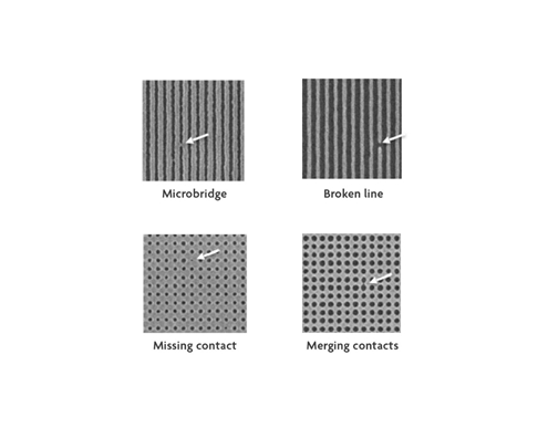
Stochastic printing failures are random, non-repeating, isolated defects such as microbridges, locally broken lines and missing or merging contacts.
Semiconductors
EUV Lithography: Weighing the Options for Future Logic and Memory Applications
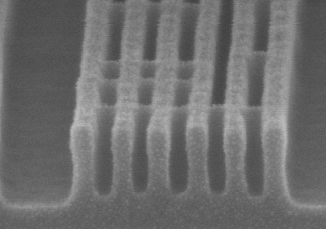
Imec takes a great leap forward in understanding and pushing the limits of extreme ultraviolet lithography – part I
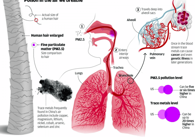
Abating Potentially Dangerous Particles 2.5 µm and Smaller
Particles, especially fine particles, are very important because of their impact on human health.
NeoPhotonics Samples High Power Semiconductor Optical Amplifiers and Narrow Linewidth Lasers for Coherent Lidar Transceivers
NeoPhotonics Corporation (NYSE: NPTN), a leading designer and manufacturer of advanced hybrid photonic integrated circuit based modules and subsystems for bandwidth-intensive, high speed communications networks, today announced that it is sampling high power Semiconductor Optical Amplifiers (SOAs) and Narrow Linewidth (NLW) Distributed Feedback Lasers (DFB) lasers for long range automotive Lidar (“light detection and ranging”) applications.
ON Semiconductor to Explore Sale of Manufacturing Facility in Belgium
ON Semiconductor Corporation (Nasdaq: ON), driving energy efficient innovations, today announced it is exploring a sale of its manufacturing facility in Oudenaarde, Belgium. The company will begin searching for strategic partners that are willing to enter into a mutually beneficial arrangement that the company expects will facilitate an orderly transition of products from its Oudenaarde facility to other facilities within the ON Semiconductor network.
SEMI-FlexTech Launches Six New Projects to Accelerate Flexible Hybrid Electronics Innovation
SEMI-FlexTech today announced the launch of six projects to accelerate sensor and sensor system innovations for new applications in industries including healthcare, automotive, industrial and defense. In collaboration with the U.S. Army Research Laboratory (ARL), FlexTech, a SEMI Strategic Association Partner, will provide more than $2.3 million in funding for the projects aimed at maturing the flexible-hybrid electronics (FHE) technology ecosystem
Surface Preparation for Low Temperature CVD Si Epitaxy Processing
Methods for producing the pristine and stable hydrogen-terminated single crystal silicon surfaces required to achieve the specifications for LT CVD epi silicon layers are investigated.
Picosun’s ALD Technology Helps to Fight Climate Change
Picosun’s Atomic Layer Deposition (ALD) thin film barrier coating technology offers a solution for eliminating the use of hazardous process gases, sulphur hexafluoride (SF6) and nitrogen trifluoride (NF3). By switching to Picosun’s ALD nanolaminate barrier technology it is possible to obtain unmatched barrier performance with extremely thin, pinhole-free films. This also eliminates the need to clean the deposition equipment after every few process runs.
Coupled Quantum Dots May Offer a New Way to Store Quantum Information
Researchers at the National Institute of Standards and Technology (NIST) and their colleagues have for the first time created and imaged a novel pair of quantum dots — tiny islands of confined electric charge that act like interacting artificial atoms. Such “coupled” quantum dots could serve as a robust quantum bit, or qubit, the fundamental unit of information for a quantum computer. Moreover, the patterns of electric charge in the island can’t be fully explained by current models of quantum physics, offering an opportunity to investigate rich new physical phenomena in materials.
NRL Researchers’ Golden Touch Enhances Quantum Technology
Scientists at the U.S. Naval Research Laboratory discovered a new platform for quantum technologies by suspending two-dimensional (2-D) crystals over pores in a slab of gold.