Smaller is better when it comes to microchips, researchers said, and by using 3D components on a standardized 2D microchip manufacturing platform, developers can use up to 100 times less chip space. A team of engineers has boosted the performance of its previously developed 3D inductor technology by adding as much as three orders of magnitudes more induction to meet the performance demands of modern electronic devices.
Semiconductors
North American Semiconductor Equipment Industry Posts December 2019 Billings
North America-based manufacturers of semiconductor equipment posted $2.49 billion in billings worldwide in December 2019 (three-month average basis), according to the December Equipment Market Data Subscription (EMDS) Billings Report published today by SEMI. The billings figure is 17.5 percent higher than the final November 2019 level of $2.12 billion, and is 17.8 percent higher than the December 2018 billings level of $2.11 billion.
Physicists Trap Light in Nanoresonators For Record Time
An international team of researchers from ITMO University, the Australian National University, and Korea University have experimentally trapped an electromagnetic wave in a gallium arsenide nanoresonator a few hundred nanometers in size for a record-breaking time. Earlier attempts to trap light for such a long time have only been successful with much larger resonators. In addition, the researchers have provided experimental proof that this resonator may be used as a basis for an efficient light frequency nanoconverter.
EV Group and Inkron Partner on High Refractive Index Materials and Nanoimprint Lithography Development
EV Group (EVG), a supplier of wafer bonding and lithography equipment for the MEMS, nanotechnology and semiconductor markets, today announced that it is partnering with Inkron, a manufacturer of high and low refractive index (RI) coating materials, to provide optimized processes and matching high RI materials for the development and production of high-quality diffractive optical element (DOE) structures. These DOE structures include waveguides for augmented/mixed/virtual reality (AR/MR/VR) devices, as well as beam splitters and diffusers for advanced optical sensing used in automotive, consumer electronic and commercial applications.

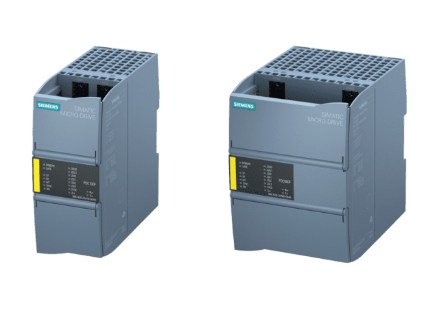
Siemens Achieves Industry-Leading Performance with GaN Systems Power Transistors
GaN Systems, the global leader in GaN (gallium nitride) power semiconductors, today announced that Siemens is integrating part of its Simatic Micro-Drive product line with GaN Systems power semiconductors. With the integration of GaN Systems power transistors, this Siemens product line features industry-leading standards and benefiting customers by power density, efficiency and robustness.
Designer-Defect Clamping of Ferroelectric Domain Walls for More-Stable Nanoelectronics
A UNSW study published today in Nature Communications presents an exciting step towards domain-wall nanoelectronics: a novel form of future electronics based on nano-scale conduction paths, and which could allow for extremely dense memory storage. FLEET researchers at the UNSW School of Materials Science and Engineering have made an important step in solving the technology’s primary long-standing challenge of information stability.
USMCA Approval Strengthens U.S. Technology and Trade Leadership
The Semiconductor Industry Association (SIA) today applauded Senate approval of the U.S.-Mexico-Canada Agreement (USMCA), which passed with strong bipartisan support earlier today. SIA represents U.S. leadership in semiconductor manufacturing, design, and research, with members accounting for approximately 95 percent of U.S. semiconductor company sales. “Congressional approval of the USMCA is a major win for free trade and America’s global leadership in semiconductors and the technologies they enable,” said John Neuffer, SIA president and CEO. “The agreement will help ensure that more products researched, designed, and made in America – including semiconductors – can flow to customers around the world. We applaud the Administration and Congress for negotiating and approving this landmark agreement.”
Synopsys Joins New Autonomous Vehicle Computing Consortium
Synopsys, Inc. (Nasdaq: SNPS) today announced that it has joined the new Autonomous Vehicle Computing Consortium. The Consortium brings together leading experts in the automotive, automotive supply, semiconductor and computing industries to help accelerate the delivery of safer and affordable vehicles. As a member of the Consortium, Synopsys will actively contribute to the development of a set of recommendations for system architectures and computing platforms that will be used to address the challenges of deploying self-driving vehicles at scale.
Worldwide Semiconductor Revenue Declined 11.9% in 2019
Worldwide semiconductor revenue totaled $418.3 billion in 2019, down 11.9% from 2018, according to preliminary results by Gartner, Inc. Intel regained the No. 1 position in the market as the downturn in the memory market negatively impacted many of the top vendors, including Samsung Electronics, the No. 1 vendor by revenue in 2018 and 2017. Intel reclaimed its position as the No. 1 global semiconductor vendor by revenue in 2019, recovering the position from Samsung Electronics, which held it for the past two years. Intel’s semiconductor revenue declined 0.7% in 2019, driven by a slowdown in the server market, an ongoing constrained CPU supply and the 4Q19 sale of its cellular modem business to Apple.
Colloidal Quantum Dot Photodetectors Can Now See Further Than Before
Optical sensing in the mid to long infrared (5microns – um) is becoming of utmost importance in different fields since it is proving to be an excellent tool for environmental monitoring, gas sensing, thermal imaging as well as food quality control or the pharmaceutical industry, to name a few. The amount of information hidden within this very rich spectral window opens new possibilities for multi or even hyperspectral imaging. Even though there are technologies that can address these challenges, they are very complex and expensive.