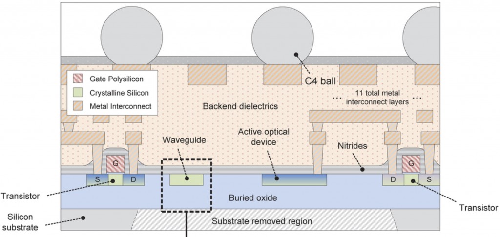
As published in the journal Nature, CMOS transistors have been integrated with optical-resonator circuits using complex on-chip sensors and heaters to maintain temperature to within 1°C. While lacking the laser-source, these otherwise-fully-integrated solutions demonstrate both the capability as well as the limitation of trying to integrate electronics and photonics on a single-chip. The Figure shows a simplified schematic cross-section of the device.

Lead author Chen Sun—affiliated with UC Berkeley and MIT, as well as with commercial enterprise Ayar Labs, Inc.—developed the thermal tuning circuitry, designed the memory bank, implemented the ‘glue-logic’ between various electronic components, and performed top-level assembly of electronics and photonics. The main limitation is the temperature control, since deviation by more than 1°C results in loss of coupling that otherwise provides for P2M/M2P transceivers:
* Waveguide Loss – 4.3 dB/cm,
* Tx and Rx Data Rate – 2.5 Gb/s,
* Tx Power – 0.02 pJ/bit,
* Rx Power – 0.50 pJ/bit, and
* Ring Tuning Control Power – 0.19 pJ/bit, so
* Total power consumption = 0.71 pJ/bit.
The Register reports that this prototype has a bandwidth density of 300 Gb/s per square millimetre, and needs 1.3W to shift a Tb/s straight from the die to off-chip memory. A single chip integrates >70 million transistors and 850 photonic components to provide microprocessor logic, memory, and interconnect functions.
—E.K.


