Thin-film transistors (TFT) created using only additive process steps could create new low-cost ICs with functionalities beyond silicon, but only if we understand how to control structures at the molecular level. Thin films of conjugated polymers such as poly(3-hexylthiophene) (P3HT) can provide useful conductivity when the electron mobilities are controlled within as well as between molecules. In producing TFTs using such organic macromolecules, we must rigorously control the deposition and annealing processes so that the right molecules line up in the right order.
Peter F. Green, Professor of Chemical Engineering, Macromolecular Science and Engineering at the University of Michigan, and his team fabricated ~55 nm thin films of P3HT using resonant-infrared matrix-assisted pulsed laser evaporation (RIR-MAPLE), as well as conventional spin-casting. The films produced by MAPLE show a higher degree of structural disorder, with localized trap sites that reduce mobility out-of-plane by an order of magnitude compared to spin-cast films.

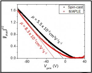
The Figure shows that despite the disorder of MAPLE-deposited P3HT, enhanced carrier density at the dielectric interface allows TFTs to exhibit similar in-plane mobilities to those built using conventionally spin-coated films. TFTs were top-contact, bottom-gate designs on 300nm thermal oxide on highly doped silicon. In-plane carrier mobilities of MAPLE-deposited versus spin-cast films were 8.3 versus 5.5 (×10 -3 cm2/V/s). In principle, the ability to independently control in- and out-of-plane mobilities allows for the fine tuning of TFT parameters for different applications.
—E.K.


