By Christine Dufour and Viraja Sharma
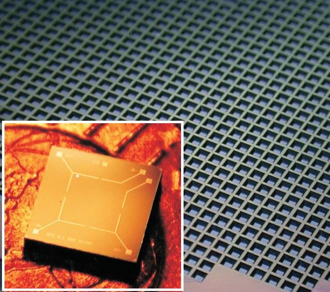
New MEMS-based products are constantly emerging, fueled by the Internet of Things (IoT), autonomous driving, smart manufacturing and healthcare applications. The MEMS pressure sensor market is no exception to this trend1. Its growth has been driven mainly by automotive applications such as tire pressure management system (TPMS) regulations in China, fuel and ignition systems, thermal systems, oil-pressure monitoring, and indoor and outdoor navigation systems. Easy to customize and integrate, miniature, sensitive, accurate and low-power MEMS devices are especially well-suited to the accuracy, power consumption, sensitivity and miniaturization that pressure sensors require.
Yet MEMS design also presents some specialized challenges, such as a strong coupling between fabrication technology and design. Complex physical structures that exhibit non-linear behavior, custom packaging requirements, and a final product that requires integration with surrounding CMOS circuitry are just a few examples. What’s more, there is a lack of standardized processes and process validation in MEMS design ecosystems.

As with other products based on MEMS technology, designers must increasingly customize pressure sensors for higher performance – sensitivity and linearity, in this case – while decreasing their package size. Designers can accomplish the task by studying sensor performance and manufacturability using computer models prior to fabrication. This can ensure that the sensor meets its required specifications while simultaneously reducing manufacturing cycles and cost.
The Power of Collaboration
This is where strong collaboration among EDA providers, MEMS technologists and designers delivers tangible benefits. EDA providers and MEMS foundries can collectively help MEMS designers to incorporate foundry process constraints into their designs.
In the semiconductor industry, first-pass successful silicon relies on standardized manufacturing processes, thorough technology characterization, accurate model generation, established simulation and verification, and extensive reuse of proven design blocks. In the MEMS world, where processes and products are developed concurrently, and processes change with every product, is it possible to adopt standardized processes, design methodologies, and tools that enable efficient reuse of existing technology and design knowledge? The challenge lies in maintaining the flexibility to optimize products for a diverse array of requirements.
The ideal design platform should ease sharing of technology and design data between the foundry and its customers, enabling two-way collaborative development and allowing foundry technologists to easily perform a feasibility assessment of a customer’s project. This approach offers important benefits, allowing designers to explore and evaluate the suitability of a foundry’s process technology in their unique application. It also supports accurate prediction of device performance prior to fabrication and reduces costly build-and-test cycles. Combining standardized manufacturing processes, MEMS process design kits (PDKs), and a proven design flow are the starting point for development of manufacturing-ready designs.
A Real-Life Example using Pressure Sensors
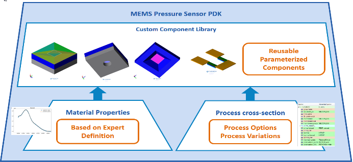
An EDA company, Coventor (a Lam Research company), along with MEMS foundry partner X-FAB, collaborated to develop a PDK that would ensure that manufacturing constraints are automatically considered early in their design process. The design flow is based upon an X-FAB fabrication platform that supports multiple process options for the manufacturing of absolute and relative MEMS pressure sensors. The PDK is a “golden container” for all the process and material characteristics of the silicon membrane and substrate, glass, passivation layers, and piezoresistive components. It enforces material properties and guarantees their correct implementation during the simulation. It also includes a component library containing ready-to-use, 3D parameterized devices (such as membranes and resistors), all pre-designed with foundry-supported materials to support their respective design rules. The components are readily partitioned for optimized meshing and simulation, saving design and simulation time.

Designers can use components from the library to create a custom design — which might include different membrane shapes and sizes, and resistors of varying shape, size and position — to simulate the impact of different technology variants (such as resistor doping profiles, membrane and substrate thickness, glass material properties, and passivation schemes). This allows them to anticipate the effect of these design changes on sensor sensitivity for varying pressure and temperature regimes.
Extensive validation of the pressure sensor design platform is currently underway. So far, the simulations have exhibited very good correlation to actual device measurements across a range of pressure and temperature conditions, including predictions of non-linear behavior for various pressure sensor designs. At the same time, the simulation accounts for mechanical membrane properties and piezoresistivity. With this type of design platform, a foundry can provide guidelines to help customers select both the fab technology and design features that lead to an optimal design solution.

Let’s Face the Next Challenges…
A complete design platform for MEMS must eventually include not only MEMS device design, but system integration functions, such as the application-specific integrated circuit (ASIC) design and packaging/assembly of the product. In addition to the design verification that the PDK provides, additional partnerships among foundries, integrated device manufacturers (IDMs), research centers, equipment suppliers, and EDA vendors will help to define requirements and solutions that address every level of design and production. These might include tasks such as describing standardized material properties and process specifications, creating accurate foundry-proven design models, and defining requirements for system-level simulation. In the future, PDK simulations might even include up to tape-out and physical verification. To learn more about this collaborative PDK development work, please click here for the whitepaper.
Christine Dufour, MEMS PDK Program Manager, Coventor
Christine Dufour is the MEMS PDK program manager at Coventor. She has more than 20 years of experience in the semiconductor industry, leading process design kit development for BiCMOS and CMOS processes at several major semiconductor companies. Ms. Dufour has also worked as a product manager in the RF design environment area. In addition to her extensive experience in MEMS PDK development, she is an expert in all aspects of MEMS design flow and design tool development. Ms. Dufour received an engineering degree at Technological University of Compiegne.
For more information on Coventor, a Lam Research Company, visit: https://www.coventor.com/
Viraja Sharma, Development Engineer, MEMS Simulation & Design, X-FAB
Viraja Sharma is a development engineer for MEMS Simulation & Design at X-FAB. Her work involves the design and simulation of MEMS inertial and pressure sensors. Prior to her tenure at X-FAB, Ms. Sharma performed similar duties for other semiconductor companies. She received her Master of Science degree in Micro and Nano Systems from TU Chemnitz, where she studied MEMS and micro technologies.
For more information on X-FAB, visit: https://www.xfab.com
Coventor and X-FAB are members of SEMI-MEMS & Sensors Industry Group that connects the MEMS and sensors supply network, enabling members to address common industry challenges and explore new markets.