
Fundamental changes are changing the value of EDA and IP, but not for the better. Will AI be the game changer?
By John Blyler, Contributing Senior Editor, Semiconductor Digest
It seems like every tech company on the planet now offers an AI application, especially in generative AI. Most are more marketing ploys than practical implementations, but all rely on specifically designed semiconductor chips. Such demand is already changing the landscape of the semiconductor industry.


These changes were the focus of the 61st DAC keynote talk by Charles Shi, Principal and Senior Analyst at Needham, LLC. His annual talk highlighted how AI is accelerating the in-sourcing of semiconductor design by systems companies. Another topic was the return of vertical integration from silicon to systems. One of the consequences of this changing landscape is that chip design is capturing a greater piece of the pie in the semiconductor value chain. This trend represents a significant opportunity for the EDA and IP industry, which he envisioned as the “pick-and-shovel” provider to the AI gold rush.
Profound Changes
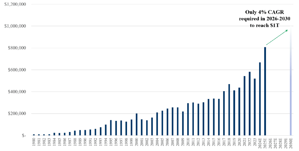
Shi began his talk by noting that the semiconductors are on track to reach $1T global sales by 2030. His confidence stemmed from the relatively low CAGR of 4% required in 2026-2030 to reach the significant $1T mark (see Figure 1).

Factors contributing to the profound changes in semiconductor growth include Nvidia replacing Intel as the new king of semiconductors in 2024. Nvidia is on course to realize estimated semiconductor sales of nearly $650M, while Intel’s estimated sales are less than half that amount (Needham).
This is significant as previous eras only sometimes had a dominant player, but the new Al era does. For example, the peak semi-market share for Intel’s x86 was ~21% in the 2000s. Arm reigned as king in the 2010s with mobile app processors used by Qualcomm and Apple. Now, in the 2020s, Nvidia’s CUDA platform currently commands ~20% of the peak semiconductor market share.
However, on a cautionary note, Shi observed that historically, the EDA segment did not do well when the industry had an “overbearing” market leader. It may be too early to tell if Nvidia will assume this role.
Design to Use
Another major change in chip design is that every hyperscaler company now has its own in-house chips, which it uses to run its data operations—shifting paradigms from “Design to Sell” to “Design to Use.”
Hyperscalers are organizations that operate large-scale data centers and cloud infrastructure to support their business operations, such as Amazon (AWS), Microsoft, Google Cloud, and Meta (Facebook). These companies can scale their infrastructure quickly to meet the growing demands of their users.
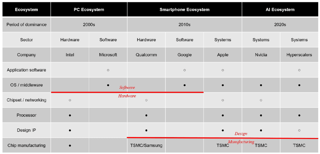
Over the last 60 years, the semiconductor value change has experienced a massive evolution, with system company IBM in the 1950s being replaced by Apple, Tesla, and nVidia in the 2010s and beyond. One result of these changes is the (re-)emergence of vertical integration, with Apple and Tesla (among others) conducting software, front-end, and back-end chip design—and even manufacturing in some cases.
Such vertical integration has caused the historical hardware/software divide to evolve into a design/manufacturing divide, again highlighting the “Design for Use” model (see Figure 2).

Not surprisingly, systems companies like Amazon, Apple, Google, Tesla, and others account for 20% of foundry revenue. Indeed, the TSMC workload also confirms the rise of systems companies in chip design.
Value Over Volume
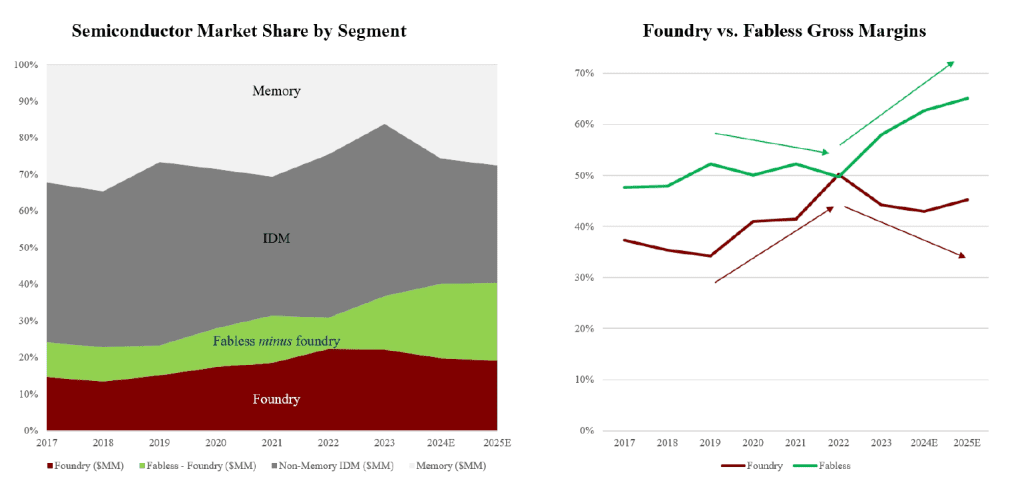
Another change is the increased focus on designers and manufacturers. The current semiconductor cycle is focused more on designers and manufacturers. More money is going to fabless design companies than foundries, and manufacturers are reporting less revenue, making cents on the dollar. Shi showed (see Figure 3) that the new semiconductor cycle is a designer’s, not a manufacturer’s.

Of course, the semiconductor ecosystem relies on both design and manufacturing. Fabless systems companies work directly with foundries like TSMC, Samsung, Globalfoundries, and others, as do the EDA and IP vendors. It’s just that the focus has shifted back to design.
Shi commented on this design shift in previous years (see link below) by addressing how innovation fits into a return to a vertically integrated value chain: “You will out-innovate through a system approach to regain competitiveness. The strength of the US is its tech ecosystem, which includes companies like Apple, Google, Microsoft, Meta, Tesla, and others. These companies will probably be the drivers of semiconductor innovation in the future. To help foster this innovation, the US should help make it easy for the US ecosystem to collaborate and innovate …”
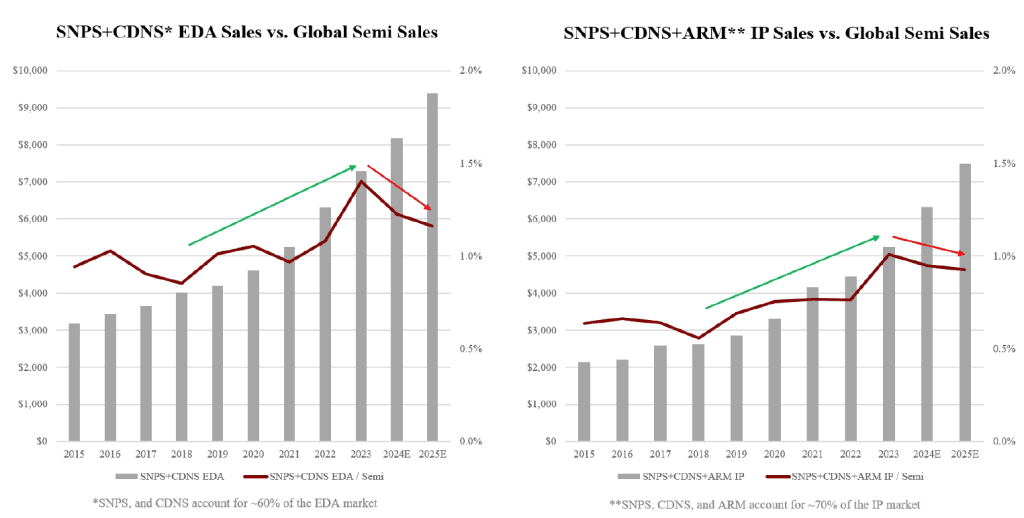
Shi then expressed significant concern about the trend, wondering if the EDA and IP industries could keep up with semiconductor growth. This was the first time he had expressed this concern in recent years. He noted that while the overall growth numbers look great, the percentage is in decline (see Figure X). This is an important point.

Transforming EDA & IP Industry
On a more positive note, Shi talked about the growth of advanced packaging, especially in the server, and now emerging in the customer systems markets. EDA tool vendors have long embraced this trend by going beyond just SOC design system-level platforms, including stacked dye packaging and PCBs.
Similarly, IP and design services have gone beyond GDS to include chiplets and more. This is part of the ongoing silicon-to-systems transition that has spread across many verticals. Of course, digital twins and AI were also mentioned in this transition.
Dickenesque Times?
Shi summarized his keynote with a play on a quote attributed to Charles Dickens’s A Tale of Two Cities: “It Is the Best of Times, It Is the Worst of Times.” Through his presentation, he characterized the semiconductor industry as experiencing the most profound changes in a decade. Nvidia (not Intel) is going to dominate the market, possibly for the next decade or two. If that past is any indicator, then the EDA industry will not fare well with only one dominant player.
Another profound shift occurs as the traditional software-hardware divide disappears, being replaced with a software-defined hardware future. Systems companies are the best positioned to drive hardware innovation in this paradigm.
To meet these challenges, the EDA and IP industries must transform themselves to play more fully in the system space. This includes increased investment in multi-die integration, as well as system-level simulation and analysis technologies. They must enable digital twins beyond just SoCs.
(Cover Photo by Jason Leung on Unsplash)