Edwards has significantly expanded in the U.S. in recent years, with a new 200,000 ft2 facility in Chandler, AZ, a state-of-the-art chemical laboratory at its Innovation Center in Hillsboro, OR and, most recently, new plans for a new dry pump manufacturing facility in Genesee County, NY. The 240,000 square-foot campus, located at the Western New York Science & Technology Advanced Manufacturing Park (STAMP), will include manufacturing, warehouse and administration.

Martin Elzingre, Vice President and General Manager at Edward Vacuum U.S., says the expansions are part of a new effort to bring products closer to their customers, easing supply chain constraints while enhancing sustainability efforts. “As part of the semiconductor ecosystem, we need to make sure we reduce our customer emissions,” he said. “We do that by constantly improving our products – moving away from fossil fuel, reducing utilities and power consumption, making them smaller, and even recycling critical gases such as hydrogen and krypton.”
The semiconductor industry has played a leadership role in coordinating worldwide action to reduce greenhouse gas (GHG) emissions, despite being a minor contributor to GHG emissions. Greenhouse gas emissions are often categorized into three groups or ‘Scopes’ by the most widely-used international accounting tool, the GHG Protocol. Scope 1 covers direct emissions from owned or controlled sources. Scope 2 covers indirect emissions from the generation of purchased electricity and other resources consumed by the reporting company. Scope 3 includes all other indirect emissions that occur in a company’s value chain.
“We’re looking at total scope 1, 2 and 3 reduction of the energy and the carbon that we produce,” Elzingre said. “We’re not just doing that by making pumps more efficient. We’re doing it by changing the materials the pumps use. We’re doing it by locating factories in places where we have low carbon energy. And we’re doing it by putting factories as close as possible to our customers and using efficient shipping methods to reduce the carbon footprint.”
Elzingre said a good example is how Edwards is to reduce methane use. “One of the big uses of methane is abatement of exhaust gases from process equipment,” he said, noting that CVD is the biggest challenges. “All of the byproducts from that are coming down the pump line and have to be either burned or diluted,” he said. “Dilution is probably not the best option because you’re still releasing it into the atmosphere.” Edwards recently introduced new abatement products that use electricity instead of methane. “The idea is to neutralize as much as the effluent from process chambers as possible with contributing the minimum amount of carbon to the atmosphere,” Elzingre said. “Most of the leading edge semiconductor manufacturers are looking to switch to an electric based abatement system.”
Earlier this year, NY’s Gov. Kathy Hochul announced that the New York Power Authority had approved 4.9 megawatts of low-cost electricity for Edwards Vacuum. “A nice thing about Genesee County, and one of the reasons we selected it, was that the energy that we’ll be using is primarily hydroelectric, so carbon- free energy,” Elzingre said.
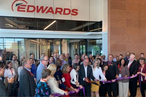
The Edwards facility in Chandler, AZ, which officially opened its doors on Thursday, April 20, 2022, features warehousing facilities, factory areas, meeting rooms, and a dedicated training center. “Unprecedented growth in the semiconductor market to meet the world’s growing consumer demand has resulted in extraordinary growth in demand for Edwards’ products and services,” said Paul Neller, President of Edwards Semiconductor Service. “Looking ahead, this growth is set to continue, with our customers in the USA investing billions of dollars in additional manufacturing capacity. At Edwards, we have a long tradition of supporting our customers with local service and manufacturing capabilities, and our investment in the Chandler facility continues that tradition. With the utilization of the latest in smart manufacturing techniques and advanced automation, this new facility will be instrumental in supporting the safe, productive and environmentally sustainable manufacturing of semiconductors in North America.”
The Edwards state-of-the-art chemical laboratory at its Innovation Center in Hillsboro, OR, announced in August of last year, provides a venue for Edwards experts to work directly with customer personnel to solve critical problems presented by rapidly changing materials and manufacturing processes. Positioning these resources close to the customer will foster early collaboration and innovation, and put safe, effective solutions into the customer’s hands faster.
“Almost everything that goes through the process chamber comes out through our equipment,” said Kurtis Fairley, Innovation Center Manager. “Mishandling those materials or allowing the wrong ones to mix can exact significant penalties, in downtime, product loss, and health and safety risks to fab personnel. The challenge only increases as the pace of development accelerates. Evaluating the impact of every new process or chemical on downstream equipment is absolutely essential. The new lab allows customers to explore these issues and develop solutions in collaboration with our experts right in their own backyard: global expertise, locally applied.”
In November of last year, SEMI announced the new Semiconductor Climate Consortium (SCC), a group formed by companies across the semiconductor value chain to accelerate the ecosystem’s reduction of greenhouse gas emissions. Edwards is one of the founding members of the consortium. The consortium’s members are committed to working toward the following pillars and objectives:
- Collaboration – Align on common approaches, technology innovations and communications channels to continuously reduce greenhouse gas emissions.
- Transparency – Publicly report progress and Scope 1, 2 and 3 emissions annually.
- Ambition – Set near- and long-term decarbonization targets with the aim of reaching net zero emissions by 2050.
- Founding members have affirmed their support of the Paris Agreement and related accords driving the 1.5⁰C pathway and are aligned on the need to drive climate progress within the semiconductor value chain. The SCC was conceptualized by companies meeting under the SEMI Sustainability Initiative, which will continue to focus on non-climate related Environment, Social and Governance (ESG) issues.
Edwards has also invested in a new building in Haverhill, Massachusetts where cryogenic service operations will be located.