New etch process that operate at cryogenic or low-temperatures (near or below -100ºC) are making it possible to create very high aspect ratio (HAR) holes needed in 3D NAND memory fabrication. Millions of holes must be etched through upwards of 200 layers with perfect uniformity. The challenge is only increasing; 3D NAND devices with 1000 layers are expected to come into play by the end of the decade or soon thereafter. 150nm wide holes with an aspect ratio of 50:1 are now routinely created in high volume manufacturing, and researchers are developing techniques to enable 100:1 aspect ratio holes.
Plasma etch works through a complex interaction of reactive ions, chemical interactions with etch gases and the material being etched (alternating layers of oxide and nitride) and etch byproducts. The trick is to optimize the etching action at the bottom of the hole while minimizing any lateral etching which would widen the hole. Fortunately, etch byproducts form a passivating layer on the sidewalls of the hole which minimizes lateral etching, so the key is to get reactive chemical species and ions to the bottom of the hole, create a reaction, and then quickly remove whatever remains.
The speed with which this can be done is largely dependent on the pumping speed of the vacuum pump. “The faster the pumping speed of the turbo pump, the faster you can pump etch byproducts out of the hole,” explains Declan Scanlan of Edwards Vacuum. “That enables you to continue etching at the bottom without stopping. It also enables you to stop building up byproducts to too high a thickness on the sidewalls.”
Edwards is now releasing a new series of turbo molecular pumps optimized to provide maximum pumping speed. Coming in a variety of sizes and configurations for maximum flexibility, these pumps provide both improved total flow capability and improved pumping speed. Another design innovation provides even larger gains in pumping speed for light gases, which potentially will become more significant as new leaner process chemistries are adopted.
The advantage of performing the etch at lower temperatures with new kinds of gas chemistries is only now beginning to be fully understood, but it’s known that, at very low temperatures, the reactions proceed by physisorbtion rather than chemisorbtion typical in conventional etching (since at lower temperatures there is not enough energy for chemisorption and the molecules physisorb). See “Developments in Cryo-cooling and Vacuum Technologies to Address Challenges of Etching HAR Features,” in the July 2024 issue of Semiconductor Digest for more details.
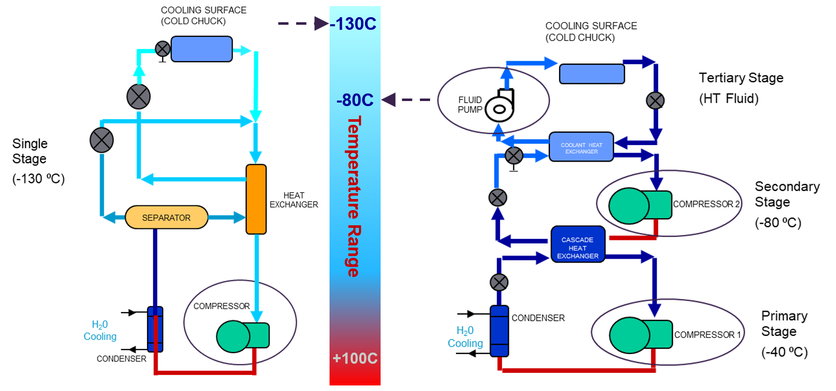
The challenge then becomes one of how to best cool the wafer and the chuck that holds it. Edwards has addressed this challenge as well, with a new cryogenic chiller called Polycold that provides cryogenic wafer chuck cooling, which will enable expanded applications by providing temperatures as low as -130°C without the use of liquid nitrogen or bulky, inefficient cascade refrigeration. Scanlan explains: “We’ve developed a unique phase separation technology that’s able to separate the gas from the liquid. You do that over a couple of cycles, and you eventually get down to just supplying the very coldest refrigerant up to the cathode, by removing off the liquid that’s already reached its boiling point.”
This means users don’t have to deal with multiple heat transfer fluids as is typical in conventional systems (see Figure). “You have one fluid mixture and one compressor. It’s just a much more efficient way to do it,” Scanlan said. “What that efficiency buys you in the end is lower energy consumption, a lower footprint and lower cost.”

