I’m delighted to turn the blog over again to Mike Czerniak, Environmental Solutions Business Development Manager at Edwards. A longtime champion of the environment, Mike, nominated by the UK Department of Energy and Climate Change (DECC), was just been accepted as the ‘expert witness’ on CF4 for the forthcoming Intergovernmental Panel on Climate Change (IPCC) working party on emissions of this extremely long-lived gas (50,000 years).
Etch Abatement Needed at 200mm Fabs to Meet WSC Goals for 2020
By Mike Czerniak, Edwards

The World Semiconductor Council (WSC) is comprised of the semiconductor industry associations (SIAs) of the United States, Korea, Japan, Europe, China and Chinese Taipei. Its goal is to promote international cooperation in the semiconductor sector in order to facilitate the healthy growth of the industry from a long-term, global perspective. Formed in 1996, the WSC early on recognized the industry’s obligation to responsibly manage its impact on the environment.
One of the council’s first acts was the issuing of a voluntary industry target to reduce the emission of perfluorinated compounds (PFC) to 10 percent below their 1995 levels by 2010. PFCs are significant greenhouse gases (GHG) and many can persist for extended periods in the atmosphere. Given the significant growth of the semiconductor industry over this 15 year period, this was a very aggressive goal. By the end of the period, all member SIAs were able to report that they had met, and in many cases, significantly exceed the stated goal. This rather impressive achievement was accomplished by two key efforts. The first was the replacement of traditional CF4 and C2F6 CVD cleaning gases with NF3, which readily dissociates in a plasma to provide fluorine, an effective cleaning gas, which, though toxic, is not a greenhouse gas. The second was the widespread adoption exhaust gas abatement.
In 2011 the industry set new targets for 2020, which it summarizes as:
- The implementation of best practices for new semiconductor fabs. The industry expects that the implementation of best practices will result in a normalized emission rate (NER) in 2020 of 0.22 kgCO2e/cm2, which is a 30 percent NER reduction from the 2010 aggregated baseline.
- The addition of “Rest of World” fabs (fabs located outside the WSC regions that are operated by a company from a WSC association) in reporting of emissions and the implementation of best practices for new fabs.
- NER based measurement in kilograms of carbon equivalents per area of silicon wafers processed (kgCO2e/cm2), which will be the single WSC goal at the global level.
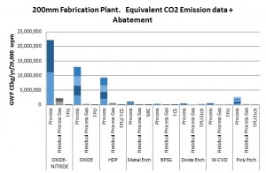
The original 2010 target focused primarily (and successfully) on emissions from chemical vapour deposition (CVD) processes. The main area for potential improvement now, as illustrated by the figure below, is etch, especially in older 200mm fabs where etch processes may not have been fitted with PFC abatement devices. This is particularly true for etch processes making extensive use of CF4, which has a very high global warming potential over a 100-year timescale (GWP100) of 7350, due largely to its atmospheric half-life of 50,000 years. It is extremely stable.

Some are predicting a prolonging of the productive lifetimes of 200mm fabs in conjunction with projected growth as a result of the growing market for internet of things (IoT). Many IoT devices do not require cutting-edge production technology and can be economically produced in older fabs. In any case, the onus is on our industry to continue our efforts to reduce any adverse effects on the environment we all share.


