Handel Jones, founder and CEO of International Business Strategies (IBS), spoke at SEMI’s Industry Strategy Symposium last week, focusing on key trends, factors impacting the growth of the industry and the migration to smaller feature dimensions. He is bullish about 2014 and industry innovation, but cautious about how quickly the industry will move to new technology nodes due to higher costs, and long design cycles. Overall, he said he believed semiconductor market growth this year will be slightly better than 2013, due in part to the strength of the global GDP.
Perhaps most surprisingly, he had a fair amount of uncertainly about 20nm. “Will 20nm be a high tech technology node and when will that occur?” he said. “We’re tracking design starts and design completions and we see a few 20nm designs but not a lot. Frankly, whether 20nm will be big or not will really depend on two customers: one is Qualcomm and the other is Apple.” Handel said “there is a significant challenge in getting lower cost at 20nm” compared to 28nm due to a lack of increase in the gate density and the potential yield impact. “We think 20nm, if it does go into volume production, it will not be in 2014. Potentially 2015 and maybe 2016,” he said.
Similarly, Handel believes there will be a postponement of 16/14nm. “We expect initial production in late 2016, beginning of 2017. That’s for the SoC business. The FPGA markets will be different,” he said. “There will also be delays in 10nm. Delays mean you can’t really go on the 2 year cycle or even the 3 year. I know people will vehemently disagree with that, but if you look at what’s really happening from a design start point of view and also the end customers, I think you’ll agree with our conclusion,” he said.
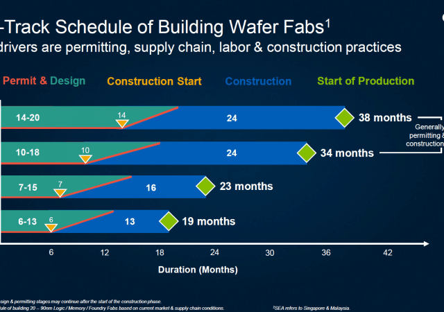
“If you look at the reality of the industry, 28nm high-k metal gate went into high volume production toward the end of 2013,” said, adding that they define high volume as 10% of the output. “It took almost 4 years for 28nm high-k metal gate to go into high volume production. Now we’re basically starting 20nm. Even if the fabs are ready what you have is the design cycle time. Preparing libraries and IP can take six months at least. Doing a complex design in 20nm can take you at least a year. Validating the design can take you another half a year. If it’s a modem, and you need approval from the carriers, that’s another half a year. Even if the fab is ready, you start these things and it’s two years,” he said. “We have an industry that is trying to adopt three technologies in three years. It’s impossible,” he said. “It’s not realistic from an infrastructure point of view, even if it the fabs are there, for three technology nodes to ramp in three years.”
Handel said that application processor (AP)/modem design can cost about $450-500 million in 16/14nm, with a timeframe of around 18 months. “You need 10X revenue so for that design, so if you’re spending $450 million, you need $4.5 billion in revenue. A few companies can get that, but not many,” he added.
“The economics of the industry are forcing changes. You’ve seen them already. The long ramp up time for 28nm HKMG, and 20nm with double patterning is clearly a major challenge from a technology point of view, and a bigger challenge from a cost point of view. FinFETs will be an even bigger challenge. Intel is having delays in their 14nm FinFETs, whether in high volume at 22nm, how will companies that have never done FinFETS before, how will design companies that have never designed in FinFETs before, how will they ramp faster?” he asked.
Not surprisingly, Handel also had a dim outlook for 10nm. He estimates that 10,000 wafers/month at 10nm will cost more than $2billion. “If you want to install 40,000 wafers/month, it’s going to be an $8 billion bill. If you want to install 100,000 wafers/month, it’s going to be $20 billion. Even before you get to 450mm, it’s going to be significantly more capital intensive,” he said.
Just looking at the location of the headquarters of semiconductor companies, he said the U.S. was still strong, but there was also strong growth from Korea – mostly in the form of Samsung – but also China and Taiwan. “We see a relatively flat Europe and then a continuing decline in Japan. In fact, we don’t see Japan strengthening unless we see some major changes,” he said.
That also has an impact in terms of the technology requirements. In terms of minimal dimensions, Handel most of the advanced technology designs are in the U.S., with advanced technology defined as being 28, 20 and now starting 16/14nm. “In developing countries, many of the designs are still at 40nm. 28 is a new technology and the next technology after 28 is going from polysilicon up to high-k metal gate,” he said.
Handel also sees uncertainly in the use of FinFET devices due to higher wafer cost. “We see quite a few new designs. The problem again is the cost per wafer. For 28nm, we have about $2600 and for 20nm we have about $3200 and for 16/14 we have about $4000. You now have this increasing cost per wafer and can you get the higher gate density and can you also get higher parametric yields?” he asked.
Handel said the gate utilization is an issue because of limitations of the design tools and parasitic effects. “The other factor is parametric yields, which are strictly tied into leakage control for the 20nm and of course for the 16nm FinFETs,” he said. “You can break this. Intel has shown that it can be broken and of course that’s an excellent achievement. But, it’s based on very high design costs, potentially $1 billion per design, so you need $10 billion in revenue. It also takes a number of years,” he said. He noted that, in the smartphone market, designs move very fast. “You can’t make that kind of investments in designs.”


I agree with 95% of Mr. Handel’s analysis.
But I do not know why all analysts forget ant FD SOI technology which gives less problems than 3-D Fin-Fet. It is more planar and gives a lot of advantages like smaller leakage, power voltage, easier designs and more control over yield.
Samsung, IBM, and Global Foundries are ahead of the others on that.
I certainly do not believe in Altera 10 nm FPGAs. First Intel must master their 14 nm yield and next 10 nm (hard to say what lithography they will use)and next Altera, a small Intel customer can benefit.
I agree 100%.
Finally, someone who isn’t connected to Intel is telling it how it really is. Forward a copy of this to David Nenni – he’ll argue all day with you.
Finally, someone not connected to Intel tells it like it is.
Send a copy to David Nenni. He’ll ague all day with you.
Arnold,
Dan Nenni’s SemiWiki also posted a near identical story. You won’t find a direct argument from him.
https://www.semiwiki.com/forum/content/3084-handel-jones-predicts-process-roadmap-slips.html
Intel is having problems with double patterning, not with FinFETs. As with the 32/28nm gate width node, Intel hasn’t used double patterning at 22nm gate width and has used 80nm first metal pitch, and is having difficulty with double patterning and 64nm first metal pitch which is required at 14nm gate width. TMSC has mastered double patterning, 64nm first metal pitch and now FinFET at 20nm gate width, and is transitioning to 16nm. FinFET seems to be by far the easier to master, and TMSC is reporting that it is ahead of programmed for 16nm volume SoC production in Q4 2014, and TMSC will be supplying Apple with 64bit 16nm FinFET SoCs for the Apple iPhone 6 in volume in Q1 2015. Intel looks it will start producing CPU chips (not SoCs) in volume about the same time.
With regard to long design cycles – yes, the design rules for double patterning makes the design of 14/16nm chips far more tedious than at 32/28nm or 22nm. However this will not stop the flagship designs from volume production in Q1 2015 – it will just mean that the ramp-up across the industry will take some time, and 32/28nm and 22nm chips will coexist for some time because of the higher cost of double patterning.
Eventual winners will be TSMC and Samsung, and then Samsung eventually. I wouldn’t be surprised if Samsung stands atop alone come 2022. TSMC has had so much trouble with its 28nm in the beginning and that has the case since then down to its 16FF. Samsung’s 28nm is rock solid as proven in A7 chips. Samsung has recruited a lot of talents of late and, trust me, what you have seen in memory space will play out exactly on logic front as well.