While much discussion has been had regarding compute and new memory types, such as high bandwidth memory (HBM), the rise of AI applications is also placing new demands on NAND storage. These applications require ever-increasing capacity to support data requirements for memory-intensive processing and AI training models.
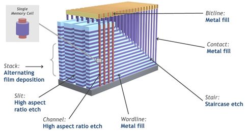
The challenge for 3D NAND manufacturers is to continue to scale density and capacity, while still delivering it at a cost that is right for the market. 3D NAND storage scaling has largely been done by stacking layer upon layer of oxide and nitride layers (ONON) and etching holes, also referred to as memory channels, through them. The nitride in the ONON stack is a sacrificial layer and is replaced with tungsten to form the word line (FIGURE 1). However, in recent years, scaling has become more difficult and complex.

“As the industry now looks towards the 1,000-layer roadmap by the end of decade or soon thereafter, there are some critical challenges. We are working actively with our leading customers to address these in time through innovations in etch, as well as other advanced manufacturing processing steps,” said Dr. Harmeet Singh, Group Vice President and General Manager of the Etch Product Group at Lam Research.
Lam has vast experience in etch, including more than 20 years as the dry plasma etch market leader and more than 10 years and 7 device generations as the NAND high aspect ratio etch market leader. “More than 100 million NAND wafers have had their memory channel created by Lam dielectric etchers,” Singh said.
The 1,000-layer HAR etch challenge
When creating 3D NAND, essentially, the number of oxide and nitride layers determines the number of memory cells and thus the memory density and capacity of the device. Each vertical memory string begins with the creation of a cylindrical hole, which might be approximately 100nm in diameter and 5-6 µm deep (an aspect ratio of 50-60:1) and penetrate 128 layers.
The difficulty of etching very deep and precise high-aspect ratio (HAR) cylindrical holes only increases with the number of layers and the corresponding stack thickness. When hundreds of layers of ONON films are patterned to create holes with a critical dimension of 100-115 nm, this pushes the etched aspect ratio (depth/width) above 100:1.
“The depth of the hole relative to its diameter is now greater than 50 to 1,” Singh said. “As vertical scaling happens, the number of layers and hole depth is increasing, but the diameter generally has been held constant.” This means that 1,000-layer 3D NAND, comprised of multiple tiers, may require a hole with an aspect ratio of as much as 100:1. “This requires that the memory channel etch have atomic precision” he said.
Creating such a high-aspect ratio hole at such small dimensions is hard to comprehend, especially when you consider that the “profile” of the hole must be near perfect from top to bottom, and, in production, a 100 trillion of them may be formed across a 300 millimeter wafer. Singh says that creating this highly precise channel shape is critical for vertical scaling, lateral scaling, and logical scaling (such as going from TLC to QLC and beyond).
“Typically, physics and chemistry would drive the bottom of this cylinder to be smaller than the top of the cylinder when we etch because there is intrinsic limitation of reactant species getting to the bottom of the feature,” Singh explained. “The cylinder has a tendency of turning into something of a cone.”
The solution
One solution to creating a perfect cylinder, says Singh, is a pulsed power plasma technology developed by Lam that uses very high power in very short bursts. “As the stack gets taller, we have been driving the ion energy higher,” he said. “The beauty of this is we have been keeping the average power constant but increasing the peak power in the pulses. This drives higher efficiency from the ions,” he said.
Lam has also employed new “cryogenic” etching, which enables the usage of a special mixture of etch gases, which in combination with other etch innovations, helps to get a near perfect profile in very high-aspect ratios holes. Cryogenic, or low-temperature etching, is a term applied to etching processes below 0°C. According to a recent paper by Lam Research, at such low temperatures there is a transition from chemisorption to physisorption, which is defined as a process in which chemical bonds are not formed upon adsorption. This leads to a higher neutral concentration on the surface and higher etching rates due to physisorption of undissociated neutral species. Enhanced adsorption of etching by-products enables profile control without the addition of polymerizing gases [1].
“The stacks have become so tall that we have transitioned and innovated in the chemistry used for cryogenic etching, and that has increased the synergy with the neutrals that are involved in the etch to get even higher etch rates than before,” Singh said.
Lam cryo etching technology — which combines high peak-peak voltage processing, cryo wafer temperatures, and process chemistry innovation — delivers 2.5x faster etch rate with 2x improvement in profile precision compared to conventional HAR etching.
Lam, which has more than 7,500 HAR dielectric etch chambers in production, was the first company to introduce cryogenic HAR etching into high volume production in 2019. More than five million wafers have been etched using Lam cryogenic processes on an installed base approaching 1,000 etch chambers.
“This has been a very fruitful journey for us. We have helped our customers transition NAND from 2D to 3D NAND, and scale 3D NAND to where it is today. Continued innovation in etch will be key to enabling the way to 1,000-layer 3D NAND,” Singh said.
Reference
1. T. Lill, et al., “Dry etching in the presence of physisorption of neutrals at
lower temperatures,” J. Vac. Sci. Technol. A 41, 023005 (2023).