Atomic Layer Deposition (ALD) has emerged as an excellent alternative to Chemical Vapor Deposition (CVD) process due to its unique characteristics, mainly conformal deposition at relatively low temperatures and excellent nanometric thin film quality from the deposition interface. Similarly, Atomic Layer Etching (ALE) is a way to remove very controlled amounts of material.
“The difference between ALD and conventional deposition is ALD uses two or more chemicals that are introduced sequentially into the reaction chamber,” explains Ben Olechnowicz, Product Manager at Swagelok. “Materials are deposited as monolayers which produces superior conformal, and consistent composition; this process of deposition of monolayer levels is repeated over and over until the desired thickness is achieved.” Surface control in ALD makes the films extremely conformal and uniform in thickness, both essential properties in emerging 3D device designs. ALD can also deposit high quality films at relatively low temperatures (150-400ºC), enabling new integration schemes and functions that would not be possible using other techniques.
An ALE process works like an ALD process, except that material is removed, instead of added, one layer of atoms at a time. “ALE is similar to ALD in that there are many minute etching steps, repeated over and over, to remove the etched material in a much more precise manner than traditional etching which is performed in a one step process,” Olechnowicz said.
The basic chemical mechanism active in ALD involves two vapor phase reactive chemical species, typically a metal precursor and a co-reactant. The precursor and co-reactant species are transported sequentially into a heated reaction zone containing a receptive growth surface, resulting in two time-separated half-reaction steps. Time-separated exposure is ensured by purging the reactor with inert gas between reactant exposure steps. Similarly, in ALE, the first chemical or plasma modifies the surface layer of atoms. Then, a second chemical or plasma turns the modified surface atoms into gas molecules that evaporate from the surface.
Valve design is key
The key to precisely controlling the chemicals used in ALD and ALE during the thousands of “on and off” steps to deposit or etch one layer is the valve design. “The valve must have capability to have multiple million cycle life; this enables the valve to be replaced at typical OEM tool preventative maintenance schedules,” Olechnowicz said.

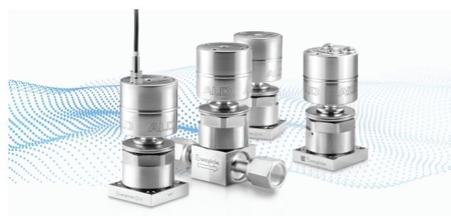
The valve needs to have very fast actuation speeds (open and close) in the millisecond range. “Even though ALD/ALE is self-limiting, OEMs still require precise chemical delivery per valve cycle (dose control per pulse) to ensure costly precursor chemicals are not wasted (vented to scrubber) but also ensure the entire area to be deposited/etched is accomplished,” Olechnowicz explained. “This is achieved through optimized valve design that provides precision actuation timing and precision valve opening/closing.”
Extreme cleanliness of the valves and other components used in ALD/ALE systems is critical. Leak-tight performance is also a must, as many of the gases used in production process fluid systems can be hazardous. “The types of chemical precursors tend to be low vapor pressure chemicals and often reactive to O2 or H2O,” Olechnowicz noted. “Since they are low vapor pressure, the valve needs to have high flow capacity as to not be a significant source of pressure drop. Also, the valve is typically heated to ensure the chemical being delivered stays in a gaseous state. With the corrosive nature of some of these precursor chemicals, the wetted material of the valve must be made from corrosion resistant materials.”
Click here to read the full article in the July issue of Semiconductor Digest.