DAVE LAMMERS, Contributing Writer
The 2024 International Electron Devices Meeting (IEDM), held in San Francisco in early December, attracted more than 2,200 semiconductor researchers, with the 2 nm logic platform presentation from TSMC as a highlight.
Speaking to a standing-room-only IEDM audience, Geoff Yeap, who led the N2 development team, emphasized the performance-per-Watt of the foundry’s N2 platform. “Technology advancement is not just about performance. It is about energy efficient compute, which is the key pillar for mobile, the AI PC, and AI processing,” Yeap said, representing more than 60 co-authors of the 2 nm platform paper.
TSMC is adopting nanosheet transistors at the 2 nm node, replacing the FinFET-based transistors employed since the 16nm node.
The NS platform hits all the full node PPA (Power, Performance, and Area) scaling metrics “at the projected cost.” Compared to the previous node, speed improved 15 percent, power by 30 percent, and area by 1.15X. With risk manufacturing already underway, the 2 nm technology will go into high volume manufacturing in the second half of 2025, Yeap said.
And the demand is clearly there. “Since the generative AI break-through moment in the first quarter of 2023, AI together with 5G advanced mobile and HPC have ignited the industry with an insatiable appetite for best-in-class advanced energy efficient logic technology,” Yeap said.
NanoFlex is TSMC’s term for mixing standard cells optimized for performance, power, or density, achieving what Yeap called “the best combination for the CPU. NanoFlex is our ability to manipulate the technology to get the highest performance at the lowest power. On blocks that are not the most performance demanding, we can use the NanoFlex (cells) to hit the power and density targets.”
In particular, the N2 transistors excel at a low operating voltage, below 0.6 Vdd.
“The energy efficiency is enhanced at low Vdd with 20 percent additional speed. The performance per Watt for the N2 technology is substantially better at a low Vdd, below .6 V.”
The N2 logic platform is “3D-optimized from end to end,” Yeap said, including a copper (Cu) RDL layer – an upgrade from the aluminum (Al) RDL layer previously used for TSMC’s 3DFabric, the foundry’s SoIC 3D-stacking technology.
The 2 nm development team improved the energy efficiency of the interconnects, particularly at the middle of the line (MoL), as shown in FIGURE 1. “Improved gate contact resistance through material and process innovation resulted in a 55 percent energy efficiency improvement, with up to 20 percent R and C (resistance and capacitance) reduction through the middle of line.”
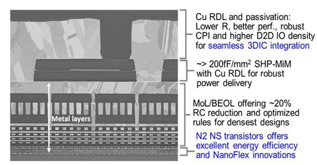
The change from aluminum to copper for the RDL metal “gives better performance. You don’t have Cu-Al-Cu, now it is all copper.”
Though SRAM scaling has stalled somewhat in recent years, Yeap said the N2 platform includes an SRAM density of 38.1 Megabits per mm squared. That compares with 32 Mb/mm2 for the N5 generation. Test chips including a GPU, Serdes, and 256 megabits of SRAM density were fabricated with “95 percent peak yields with no repair,” he said.
Smart phones as “personal assistants”
In a Sunday Short Course on the future of logic, TSMC senior director Lipen Yuan gave his view of how the semiconductor industry will reach a trillion dollars in revenues in 2030. “In every decade, a new innovation has come along to take the industry to new levels. At every step came an innovation, with AI taking off in late 2022.”
“Energy efficiency in AI is king; it is driving all our decisions at TSMC. Energy is as important as performance now,” said Yuan, senior director of advanced technology business development at TSMC.
GPUs and other devices have boosted the High Performance Computing (HPC) segment, with Yuan citing a compound annual growth rate (CAGR) of 73 percent for chips used in AI servers. Nvidia’s Blackwell GPU, made on TSMC’s N4P (4 nm) process, has a gate count of 104 billion transistors, while AI also has propelled High Bandwidth Memory (HBM3e), network switching silicon, and multi-chip packaging.
Though most of the semiconductor industry’s growth last year (2024) came from the HPC/AI sector, Yuan said AI will be behind respectable growth rates returning for PCs, smart phones, robots, and autos. PC processors must handle increasing inference processing workloads with powerful NPUs (neural processing units). Smart phones empowered with AI inference processing will become our “personal assistants, learning our unique behavior,” Yuan said, stimulating 4X growth in the Gen AI smartphone sector between 2024 and 2028.
By 2030, 90 percent of cars will incorporate autonomous driving (ADAS) capabilities. “AI will transform the automotive experience,” Yuan said.
FinFET Vt variation explodes
Leading edge logic transistors are moving to gate all around (GAA) architectures because FinFETs have run out of gas (FIGURE 2). Victor Moroz, a senior fellow at Synopsys, explained that fin width is defined by litho/etch, with ~0.6 nm at 1*sigma of variability. “This variability prevents scaling the nominal fin width below ~5.5 nm to avoid getting below dangerous (pattern collapse) territory of under ~3.5 nm.”
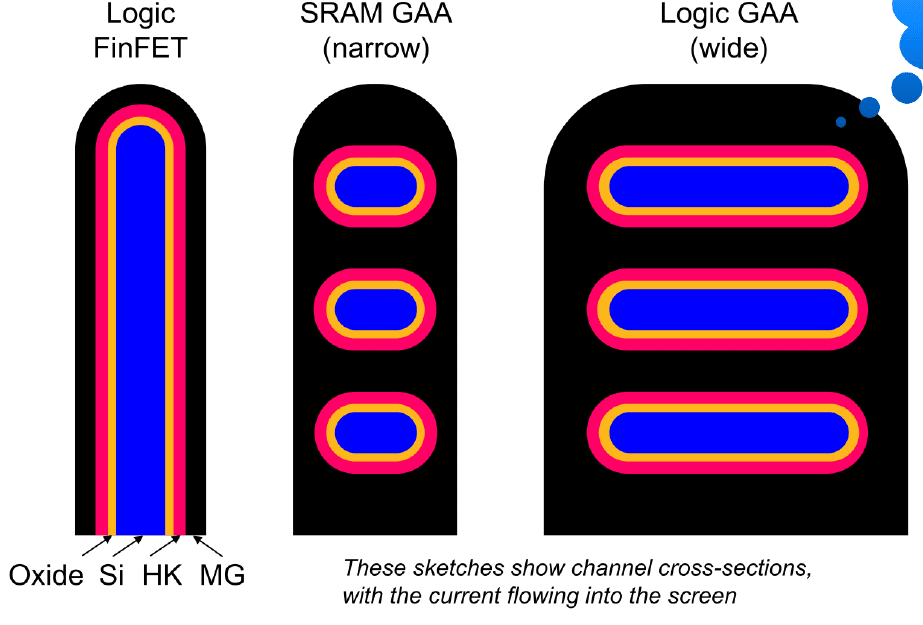
In contrast, GAA channel thickness is defined by the more precise epitaxial process, with 1*sigma of less than 0.2 nm variation. Also, threshold voltage (Vt) is increasing with fin width scaling due to the band gap widening – “a purely quantum effect.” GAA transistors have a tighter Vt variation due to the better channel thickness control by epi instead of litho-etch, Moroz said.
A presentation by Ashish Agrawal, a senior researcher at Intel Foundry, noted that the nanosheets “confine the channel from all four directions.” In one sense, he said “there is no scaling beyond nanosheets. NS is the architecture of choice for stacked FETs, and even 2D material channels.”
Agrawal focused on taking nanosheet transistors beyond the best-reported-to-date gate lengths, and to a previously unreported 3 nm nanoribbon channel thickness (Tsi) with no degradation of electron mobility. At the 6 nm gate length, the Intel research team optimized the source and drain junctions and doping profile to achieve the best performance and short channel effects (SCE). The nanoribbon thickness played a major role in controlling the drain induced barrier (DIBL) and other performance limiters. At thinner channels, beyond 3 nm Tsi, surface scattering phenomenon degraded transport.
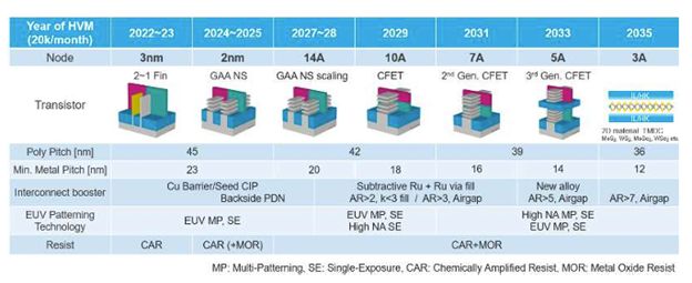
At IEDM, TSMC researchers reported using CFETs to build “the first fully functional 3D monolithic CFET inverter at an industry-leading 48 nm contacted poly pitch.” The researchers stacked n-FET-on-p-FET nanosheet transistors, with backside contacts and interconnect for improved performance and increased design flexibility, said S. Liao. FIGURE 3 shows a roadmap through 2035 and the introduction of CFETs.
Backside power delivery
The backside of wafers and devices is like a previously undeveloped continent for advanced logic researchers, albeit with significant process complexity. Anne Vandooren, Principal Member of Technical Staff at imec in Belgium, gave a presentation describing a CFET device with a backside power delivery network and backside contacts. By using SOI wafers, wafer bonding, and backside bottom dielectric isolation (BDI) the number of standard cell tracks was reduced to four from five.
Access to the wafer back side (BS) is enabled by aligned fusion bonding of a carrier wafer to a device wafer at low temperatures (<250°C), resulting in void-free bonding with high bonding strength, Vandooren said.
The advantage of CFETs is that device density improves as the NFETs and PFETs are stacked vertically, using a common gate in many cases. In her presentation, Vandooren detailed the process steps required for two different processing flows, with the BDI approach delivering the best performance. “While requiring more complex processing, the BDI approach provides excellent isolation with higher tolerance to contact misplacement and full suppression of substrate leakage current.”
In her short course presentation on the future of logic, Anupama Bowonder, principal engineer, process technology development at Intel Foundry, said the added complexity of vertically stacking devices (CFETs) ensures that the nanoribbon architectures will be refined, generation by generation, over the next decade. Bowonder outlined the challenges of moving to CFETs, including alignment, bonding, thermal budgets, and ensuring that electron and hole mobility are “comparable.”
“For monolithic CFETs — stacked N and P — we need to motivate people this is where the industry is headed,” she said, adding that with new stacking concepts, the industry will still be able to deliver gains in performance and reliability.
“Moore’s Law is alive, ever alive; CMOS scaling is definitely not dead,” Bowonder said.