Brian Krzanich, chief executive officer of Intel, said Intel is standing firm on 450mm development (despite rumors to the contrary), during a quarterly conference call with financial analysts. He also blamed defects on a slight push-out of next-generation 14nm technology.
When asked about 450mm plans, Krzanich said: “We have not changed our timing. We are still targeting the second, latter half of this decade. We continue to see great value in 450. It brings tremendous economic value to everybody who participates in it. We continue to work with our partners. We are here part of the joint development program in New York, continuing to work on 450. We continue to work with our partners, especially TSMC and Samsung and we are still targeting the back half of this decade. This is a long 10-year program when you really take a look at it. So I think you will get mixed signals throughout those 10 years,” he said.
As noted in my last post, progress is on track at the G450C consortia — an initiative by five big chip makers, Intel, TSMC, GLOBALFOUNDRIES, IBM and Samsung, partnered with New York state and CNSE — to develop 10nm capability on 450mm wafers in 2015 or 2016.
Krzanich also commented on the status of the firm’s 14nm roll out. “We continue to make progress with the industry’s first 14nm manufacturing process and our second generation 3D transistors. Broadwell, the first product on 14nm, is up and running as we demonstrated at Intel Developer Forum, last month. While we are comfortable with where we are at with yields, from a timing standpoint, we are about a quarter behind our projections. As a result, we are now planning to begin production in the first quarter of next year,” he said.
When asked about why the delay, Krzanich said it was “simply a defect density issue,” and said it was just part of the development process. “As we develop these technologies, what you are doing? You are continually improving the defect densities,” he said. “As you insert a set of fixes in groups, you will put four or five, maybe sometimes six or seven fixes into a process and group it together, run it through and you will expect an improvement rate occasionally as you go through that,” he said. He said the fixes don’t deliver all of the improvements. “We had one of those,” he said. “Why do I have confidence? Because, we have got back now and added additional fixes, gotten back onto that curve, so we have confidence that the problem is fixed, because we have actually data and defects and so that gives us the confidence that we are to keep moving forward now.”
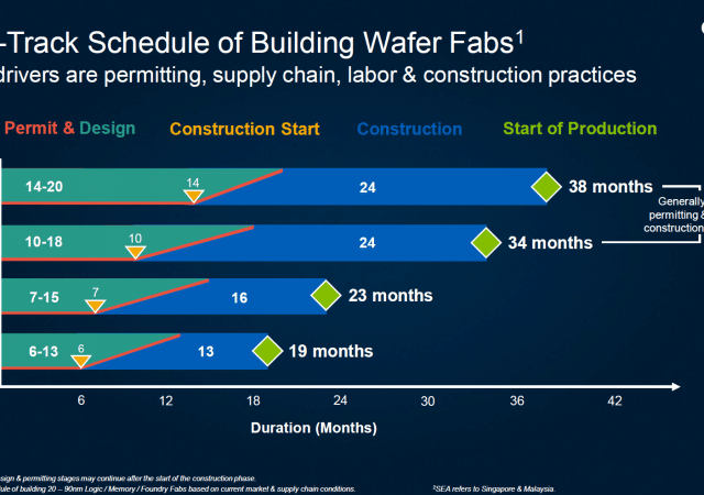
Intel has already started construction on a 450mm pilot line at its Ronler Acres location on Northwest Highway in Hillsboro. The D1X module 2 is about the same size (1.1 million square feet) as the original fab D1X and is built specifically for 450mm wafers. When the second module is complete, it will start up on 450mm wafers once it is equipped with appropriate manufacturing tools and gear.
Intel is currently equipping its D1X development fab to process 300mm wafers using 14nm manufacturing and expects to initiate production this year. While the D1X module 1 facility is 450mm-capable, it will come online as a 300mm fab.

TSMC is the only other company with an effort underway to develop a 450mm production facility. In June 2012 it was reported that the Taiwanese government had approved a proposal to build a 450mm wafer fab in central Taiwan early in 2014. TSMC said back in 2011 that it planned to install 450mm pilot lines within a couple of established wafer fabs — Fab 12 in Hsinchu and Fab 15 in Taichung, Taiwan.


Due to the delay of Intel’s 14nm FinFET manufacturing to the first quarter of 2014, TSMC’s first 16nm FinFET will be the most advanced process technology to be manufactured below Intel’s 22nm node in the 4th quarter of 2013. The device electrical transfer characteristics to be presented at the IEDM look impressive, and will be very interesting if Intel’s 14nm FinFET data could be published for a comparison.
Due to the delay of Intel’s 14nm FinFET manufacturing to the first quarter of 2014, TSMC’s first 16nm FinFET will be the most advanced process technology to be manufactured below Intel’s 22nm node in the 4th quarter of 2013. The device electrical transfer characteristics to be presented at the IEDM look impressive, and will be very interesting if Intel’s 14nm FinFET data could be published for comparison.
It is amazing that companies like Intel are pushing the limits of semiconductor technology in terms of reducing the transistor size and increasing the wafer size. I wish all the success to Intel.
By the standards TSMC is using for production, Intel has been in 14 nm production for probably a year. 1st quarter of 2014 is mass production of MPUs. No one has even taped out 16 nm finFET products yet (according to TSMC).
I don’t think it is fair to compare Intel and TSMC’s as the two companies are pushing very different aspects of logic technology. TSMC is producing mostly general purpose processes for shrinking dies size. Intel is pushing the performance for processors with random logic, memory, pll, power management etc. There is a big difference in the deliverables the only commonality may be wafer size!
Is it truly a 14nm half pitch process or is this the equivalent expected planar process performance? Since the process technology is FINFET is the half pitch LW physically greater than 14nm?