César Javier Lockhart de la Rosa, Program Manager Exploratory Logic at imec, and Gouri Sankar Kar, VP of Compute & Memory Device Technologies at imec
It has been clear for nearly two decades that the pure dimensional scaling inspired by Moore’s Law is no longer the only indicator to predict the evolution of CMOS technology nodes. The first sign came around 2005 when node-to-node performance improvements at fixed power – referred to as Dennard scaling – started to slow down. Gradually, the semiconductor industry started to complement lithography-centric scaling with other technology innovations to maintain the performance-power-area-cost benefit: material and architectural explorations at transistor level, design-technology co-optimization at standard cell level, and system-technology co-optimization enabled by 3D integration technologies.
At transistor level, the scaling-induced performance degradation originated from short channel phenomena. The combination of strong gate length reduction and the shortening of the conduction channel led to an increase in leakage current, even when no voltage was applied to the gate. Similarly, the impact of source and drain on the shrinking channel region grew dramatically.
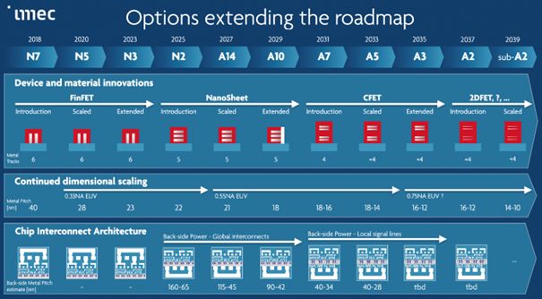
These short channel effects drove the chip industry to transition from planar MOSFET to FinFET, and recently, to gate-all-around (GAA) nanosheet transistors for high-performance computing applications. These architectural innovations allowed the gate to regain electrostatic control over the conduction channel. The nanosheet family of transistors promises to continue the logic scaling roadmap with at least three technology generations, when combined with innovations at standard cell level. These include, among others, advanced interconnect and middle-of-line schemes and the introduction of backside power delivery networks (BSPDNs).
The complementary FET or CFET will be the next game changer, allowing further area reduction by stacking n and p channels on top of each other. Imec foresees its introduction from the A7 node onwards, extending the imec technology roadmap to at least the A3 generation. Just like in GAA nanosheet transistors, the gate – now common to n and p – fully wraps around and in between the Si channels, ensuring maximal electrostatic control.
Enter: 2D materials
But eventually, even in the CFET transistor era, short channel effects will again complicate further scaling. The continuous reduction of the transistor’s gate and channel length requires ever thinner semiconductor channels to restrict the pathway for the current to flow, hence limiting the opportunity for charge carriers to leak when the device is turned off. To move CFET transistors into the A2 transistor technology node with conduction channel lengths below 10nm, the Si channel’s thickness should also shrink below 10nm. But in such thin Si channels, the mobility of the charge carriers and the transistor’s on-state current begin to decline dramatically.
That’s where 2D semiconductors, more particularly, transition metal dichalcogenides (MX2), provide an opportunity (FIGURE 1). In these semiconductors, atoms are arranged in layered crystals with a single layer thickness of only ~0.7nm, allowing for very thin channels. In addition, they promise to maintain a relatively high carrier mobility independent of channel thickness. This enables ultimate gate and channel length scaling without worrying about short channel effects.

2D material integration in advanced nodes: challenges
The big performance leap that 2D channel materials can deliver at ultimately scaled nodes has sparked the interest of major chip manufacturers and academic leaders in the field. Encouragingly, they have started to invest heavily in research and development to overcome the obstacles of introducing 2D materials in the most advanced nodes. 2D-material integration indeed comes with its own set of challenges, adding to the cost and integration efforts towards A2 node introduction.
Click here to read the full article in Semiconductor Digest, including new updates from IEDM.