At SEMI’s 2020 Industry Strategy Symposium (ISS), held January 12-15th at Half Moon Bay in California, Marco Pieters, Vice President, EUV Product Marketing, ASML provided a status report on EUV’s acceptance in high volume manufacturing and an update on progress toward the company’s next-gen high NA tool.
EUV (extreme ultra-violet) lithography offers significant advantages in terms of reducing process complexity by eliminating the need for multi-patterning. This results in major cost savings. Pieters said that EUV finally made it into high volume production last year, with multiple companies announcing chips that had been produced with EUV. “That was a significant milestone for us in the EUV program, where we have spent almost two decades developing this technology,” Pieters said.
With some assistance of some animation, Pieters showed how EUV creates light by vaporizing small droplets of tin, around 30 microns in diameter, with a CO2 laser. “Every droplet is hit twice in order to get the maximum amount of EUV from the source vessel into the scanner. When we do this for high volume manufacturing, we do it 50,000 times per second, 24/7.“
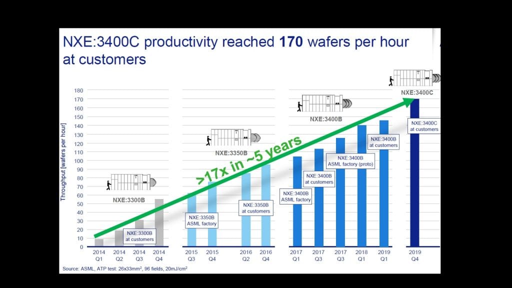
Pieters showed how productivity has improved, noting a 17X improvement in the last five years to reach 170 wafers per hour (Figure 1). “We start this graph in 2014 because prior to that we were not talking about wafers per hour, but hours per wafer,” Pieters joked.

Progress has also been made on imaging and overlay performance. “Once you have the perfect image of a layer, then you also have to make sure that you’re able to stack all these layers on top of each other. You have to interconnect 80 to 100 layers with nanometer precision and for high volume manufacturing it means you have to do that 24/7 across thousands of wafers per day,” he said.
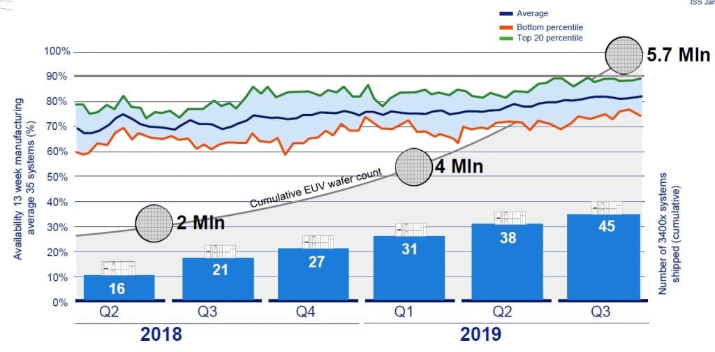
Figure 2 shows the number of 3400x EUV shipped over the last two years, along with uptime. “We have increased the uptime of the EUV system to about 80%, and if we look at the top 20% across all systems, we’ve actually achieved already 90%,” Pieters said. The goal is to increase the overall uptime to above 90%. In the middle of 2018, about two million wafers had been passed through EUV systems. “At the end of Q3 last year, this was already approaching six million,” he added. He believes that number will grow to over 20 million this year.

Pieters said ASML is currently working on a new EUV that has a higher numerical aperture (NA), moving from 0.33 in today’s scanners to 0.55. This will require advances in mask absorbers and resists. “With advanced mask absorbers, such as high-k masks, you can sustain a good imaging contrast all the way down 12 nm. If you then switch to the 0.55 NA, you can continue scaling all the way down to 8nm,” he said. Resists have improved by a factor of two in the last six years, but further improvement is needed, he added.
Also to be introduced in the platform is a new generation of stages. “We are making major steps in speed and accuracy to maintain the right overlay and focus performance and not sacrificing productivity,” Pieters said. “We’re not only increasing the acceleration, but we have to make sure that we can position this thing at any given moment in time, below a nanometer in accuracy.”
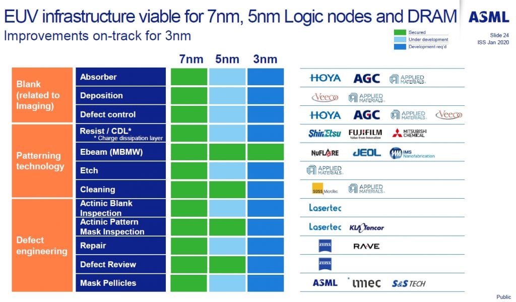
Pieters said the dose is “very viable” for 5nm processing, but improvements are needed for the 3nm node when it comes to blanks, patterning technology and defect engineering. Figure 3 provides a snapshot of various EUV-related projects and their status.

“The extension of logic-scaling beyond the next decade is possible thanks to the extendibility of EUV, including high-NA, but has to be combined with also progress in resists, in masks, to basically maintain the overall contrast and prevent productivity loss,” Pieters said. “We all have to work together to make this happen.”
Also see:
