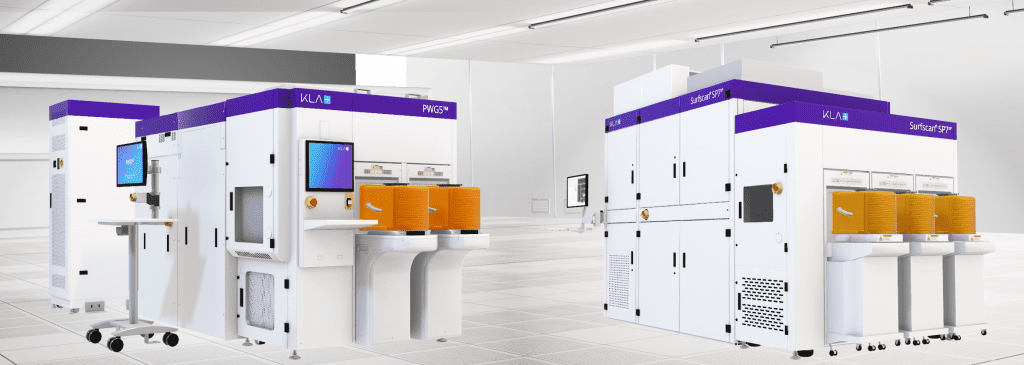
Today KLA Corporation (NASDAQ: KLAC) announced two new products: the PWG5™ wafer geometry system and the Surfscan® SP7XP wafer defect inspection system. The new systems are designed to address exceedingly difficult issues in the manufacture of leading-edge memory and logic integrated circuits.

Stacked ever higher, like molecular skyscrapers, the most capable flash memory is built in an architecture called 3D NAND. Today’s 96-layer top-of-the line memory chips, already on the market in the most advanced mobile devices, will soon be superseded by 3D NAND structures with 128 or more layers in the ongoing quest for increased space-efficiency and cost-effectiveness. To manufacture these complex structures requires depositing hundreds of thin films of multiple materials, and then creating memory cells by etching and filling holes several microns deep and one-hundredth of a micron across. As these film stacks grow higher, they induce stress on the wafer, ultimately distorting the surface planarity of the wafer. These warped wafers impact the uniformity of downstream processes and patterning integrity, ultimately affecting final device performance and yield. The PWG5 metrology system can measure minute distortions of wafer geometry with unprecedented resolution to identify and correct patterned wafer distortion at the source. Moreover, these critical wafer geometry measurements can now be accomplished for large warp ranges at inline speeds.
“The complex multilayer construction of 3D NAND has moved wafer geometry measurements to the forefront,” said Jijen Vazhaeparambil, general manager of the Surfscan and ADE division at KLA. “Our new patterned wafer geometry system, the PWG5, has the sensitivity to measure any deviations from planarity on the front side and back side of the wafer simultaneously. Its first-of-a-kind inline speed and exceptional resolution support not only 3D NAND, but also advanced DRAM and logic applications. Coupled with KLA’s 5D Analyzer® data analytics system, the PWG5 helps our customers drive decisions, such as wafer re-work, process tool re-calibration, or alerting the lithography system so that best possible patterning corrections can be applied. The PWG5 system plays a critical role in process control, helping grow advanced memory and logic yield, performance and fab profitability.”
On the leading-edge logic side of the semiconductor industry, high volume manufacturing of 5nm node devices is rising while the 3nm node is under development.* EUV lithography has become nearly universal for the most critical layers within these nodes, and device manufacturing is further complicated by novel geometries like finFET or gate all around (GAA) transistor architectures. Patterning such small, complex features in a repeatable way, billions of times across a wafer, requires exquisite defectivity control, including use of unpatterned wafer inspectors for careful qualification of starting substrates and materials, and frequent monitoring of processes and tools. The new Surfscan SP7XP unpatterned wafer defect inspection system features advancements to sensitivity and throughput, and introduces machine learning-based defect classification that together enable capture and identification of an even wider range of defect types on an even wider range of blanket films and substrate types than the benchmark Surfscan SP7.
Vazhaeparambil added, “The Surfscan design team focused not only on technical advances to support sensitivity and defect classification, but also on improving the cost of ownership.” As a result, the Surfscan SP7XP represents a single-tool solution for unpatterned wafer inspection applications from R&D to high volume manufacturing of leading-edge design node substrates and devices. It is in use at silicon wafer manufacturers, semiconductor equipment manufacturers developing defect-free processes, and semiconductor fabs for ensuring incoming wafer, process and tool quality.
To maintain their high performance and productivity, Surfscan SP7XP and PWG5 systems are backed by KLA’s global comprehensive service network. For more information about the technology advances that enable the PWG5 and Surfscan SP7XP systems’ new capabilities, and to read about applications of the systems beyond those described here, visit the KLA Advance newsroom.