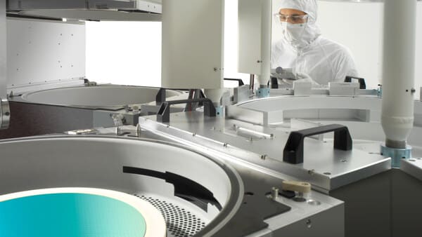
Lam Research Corp. (Nasdaq: LRCX) today announced the donation of its innovative multi-chamber semiconductor etching system to the Marvell Nanofabrication Laboratory at the University of California, Berkeley to advance research and development (R&D) for next-generation chip technologies. Through Lam’s donation, frontline researchers can now have access to a state-of-the-art etching system for fabricating nanoscale semiconductor devices, including Specialty Technologies, that are needed to support a wide range of applications — from consumer and industrial electronics to artificial intelligence (AI) and quantum computing hardware.
The Berkeley Marvell NanoLab is a shared research center providing cross-departmental principal investigators and hundreds of academic and industrial researchers with access to micro- and nano-fabrication technologies typically only found in modern fab facilities. Lam’s latest contribution builds on the company’s long history of collaboration with UC Berkeley to expand research and educational activities in nanoscale science and engineering to accelerate the pace of innovation for semiconductor manufacturing.
“We believe that academia-industry collaboration is crucial to driving the nanofabrication advancements needed for new generations of Specialty Technologies,” said Vahid Vahedi, chief technology and sustainability officer at Lam Research. “Lam’s donation will give UC Berkeley’s NanoLab researchers the ability to work directly with an industry-proven semiconductor manufacturing system in their efforts to accelerate innovation and develop new, novel processes.”
The system combines Lam’s Kiyo® conductor and metal etch, Flex® dielectric etch, and a state-of-the-art Syndion® GP deep reactive ion etch chambers on a Lam 2300® platform. It is capable of etching a broad range of materials needed for manufacturing next-generation semiconductor devices and advancing Specialty Technology applications such as optoelectronics and photonics, sensors and radio frequency (RF) solutions.
In addition to Lam’s donation, the company’s ongoing collaboration with UC Berkeley includes funding of foundational research within the College of Engineering. Lam’s etch technologies will enable expanded pathfinding in new fabrication processes for integrated optical solutions such as switches, waveguides, electro optic modulators and fiber coupling technologies. Such optical elements are critical building blocks in the advancement of photonic integrated circuits and optical interconnects, solutions that are expected to serve as critical enablers for applications including optical communications, advanced AI hardware, data center infrastructure and quantum information processing.
“We thank Lam Research for its many contributions over the years to UC Berkeley’s Marvell NanoLab in support of research and innovation for nanofabrication technologies,” said Tsu-Jae King Liu, dean of UC Berkeley’s College of Engineering. “Lam’s latest donation gives our researchers and students access to wafer-processing capabilities rarely accessible outside of the most sophisticated semiconductor manufacturing facilities. I look forward to seeing Lam’s advanced etching system enable new atomic-scale innovations for next-generation chips in the years ahead.”
As one of the founding industry members of the Berkeley Emerging Technologies Research (BETR) Center, Lam continues to support semiconductor R&D at the university where it has an endowed Lam Research Distinguished Chair in Semiconductor Processing.
