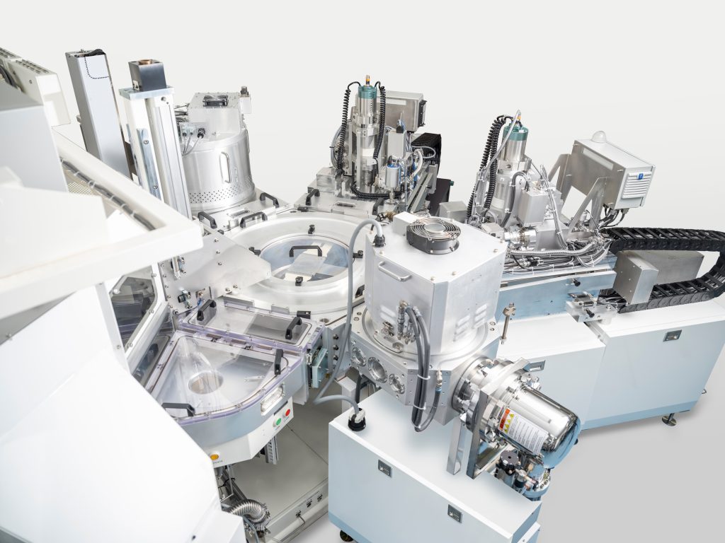
Lam Research Corp. (Nasdaq: LRCX) today introduced the world’s first production-oriented pulsed laser deposition (PLD) tool to enable next-generation MEMS-based microphones and radio frequency (RF) filters. Lam’s Pulsus PLD system delivers aluminum scandium nitride (AlScN) films with the highest scandium content available. This paves the way for advanced consumer and automotive devices with enhanced performance, capability and functionality. Pulsus is now shipping to select specialty device manufacturers.

The addition of Pulsus PLD to the Lam portfolio further expands Lam’s comprehensive range of deposition, etch and single-wafer clean products focused on specialty technologies and demonstrates Lam’s continuous innovation in this sector.
“Lam leveraged deep expertise in specialty semiconductor technologies, proven capabilities in deposition, and a strategic collaboration with CEA-Leti to bring this game-changing solution to customers on our production-proven 2300® platform,” said Chris Carter, group vice president and general manager of the Customer Support Business Group at Lam Research. “This new deposition technique can help advance device designs and accelerate product roadmaps in the specialty market.”
Cutting-Edge Films Drive High Performance Devices
RF filters play a critical role in 5G, WiFi 6 and WiFi 6E performance by increasing the number of bands a network can handle while also improving each user’s experience. MEMS microphones are valued for a high signal-to-noise ratio that allows them to capture even muffled sounds accurately — essential for voice control features and noise cancellation in 5G-enabled devices.
Pulsus uses breakthrough technology to deposit high-quality films that optimize RF filters and MEMS microphones. The higher the scandium level in the film, the better the performance of the devices. Pulsus delivers films composed of at least 40% scandium — the highest concentration available today. These films feature low dielectric loss and twice the piezo coefficient of current sputtered films, optimizing electrical conversion to drive enhanced sensitivity in RF filters and better performance in MEMS microphones. Further, improved piezoelectric qualities make it feasible to replace lead zirconate titanate (PZT) with lead-free AlScN.
In Pulsus’ PLD process, an intense laser pulse is used to strike a target material. The target is vaporized, creating a stable, dense plasma plume that is deposited in thin layers onto a wafer. This process is vital for achieving high-quality, uniform films with precise control over thickness and stress. Pulsus represents the first time lasers have been used for thin film deposition in high-volume manufacturing.
Pulsus Provides Unique Benefits for Specialty Technologies
“Demand for manufacturing equipment used to make MEMS devices grew to over $940M in 2023 and could keep growing as chipmakers find new ways to improve device performance. The superior film quality of Pulsus holds tremendous value for 5G applications that require strong piezoelectric performance,” said John West, deputy director of manufacturing and global supply chain at Yole Group. “Pulsus is an innovative solution to help optimize specialty devices now and advance technology roadmaps for varied applications to come.”
The PLD capabilities of Pulsus, supported by Lam’s 2300 platform design, ensure exceptional film uniformity and quality at a fraction of the cost per wafer versus conventional deposition methods. This efficiency can help chipmakers boost manufacturing yields and accelerate their product roadmaps.
In addition to AlScN, Pulsus can deposit a wide range of complex, multi-element materials that cannot be applied by other methods. Lam is exploring new materials to meet the demands of the specialty technology market for applications such as AR/VR and quantum computing.
“The Pulsus PLD system is unique in its ability to deposit numerous materials, including AlScN, with outstanding thin film properties,” said Sothachett Van, head of investment and supplier partnership group, CEA-Leti. “We are excited to see this technology mature into a high-volume manufacturing solution for piezoelectric MEMS devices.”