DR. SREEKANTH CHIRAYATH, IPG Laser GmbH & Co. KG. Germany, part of the global IPG Photonics Corp.
An increasingly urgent industry topic is the realization of sustainable manufacturing improvements to fulfill environmental imperatives and NetZero goals. A particular area of opportunity is wafer heating, which is common in annealing, epitaxy, etching, deposition, and bonding processes. Laser heaters show promise to impact sustainability in numerous ways, ranging from increased tool efficiency, shorter process cycle time, and lower maintenance and consumables burdens associated with thermal processing, all of which lighten the impact of a process on fab infrastructure.
We demonstrate and model a wafer heating concept based on near infrared (IR) laser illumination on 200 mm silicon (Si) wafers. Our findings suggest that wafer heating by laser offers attractive energy and cycle time savings. The same IR heating laser has already proven its effectiveness in lithium-ion battery cell manufacturing and in curing powder coat, while delivering the extraordinary energy efficiency and throughput benefits proposed here for chip-making.
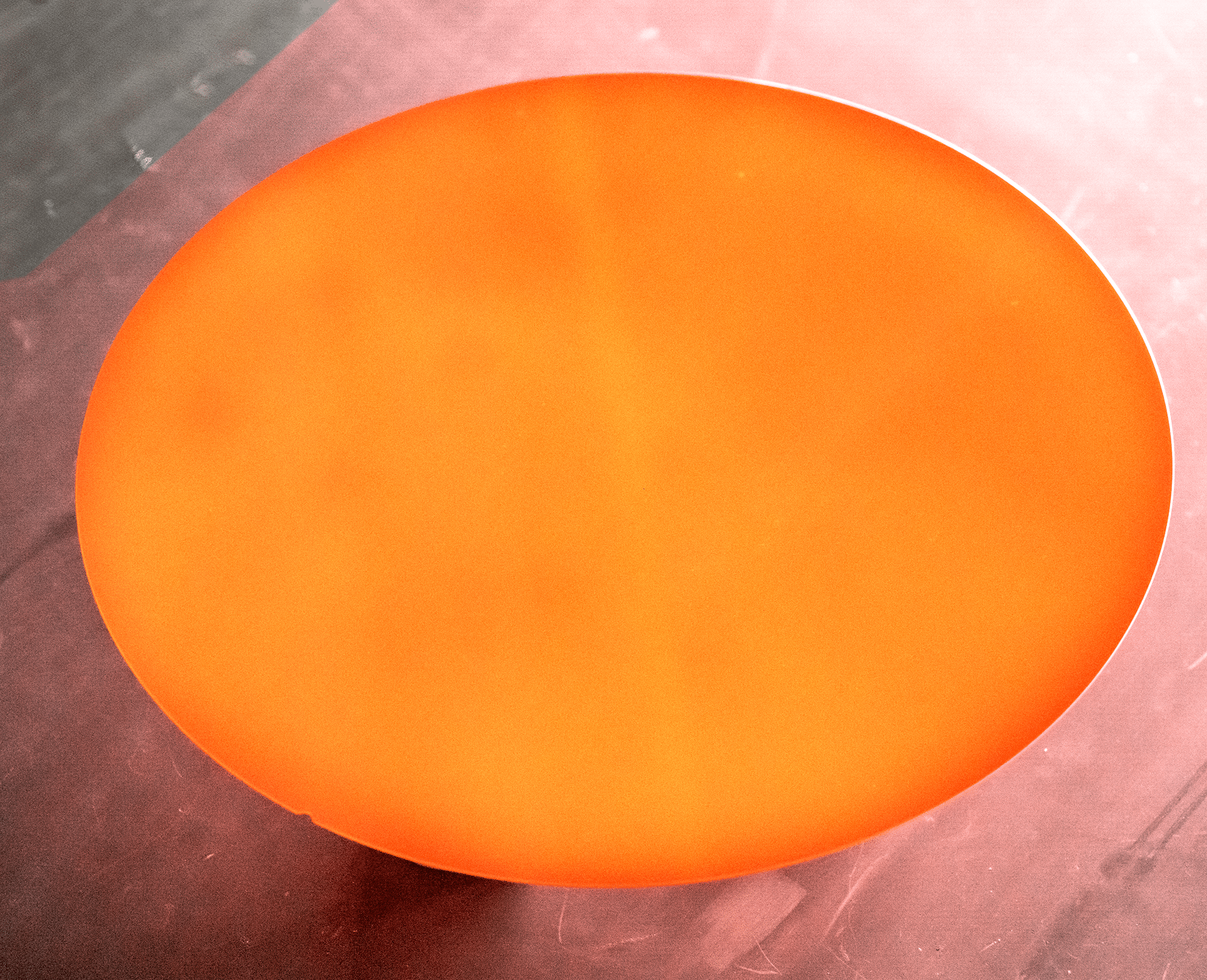
Here is a link to a video demonstration of a laser wafer heater where a 200 mm Si wafer is heated to 800°C in less than 9 s using an 8.1 kW near-IR DLS-ECO laser from IPG Photonics.
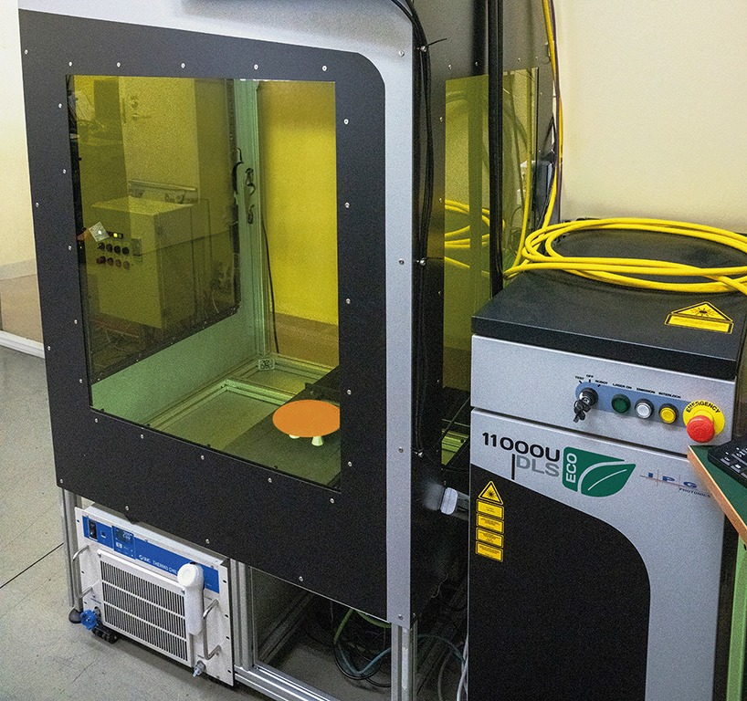
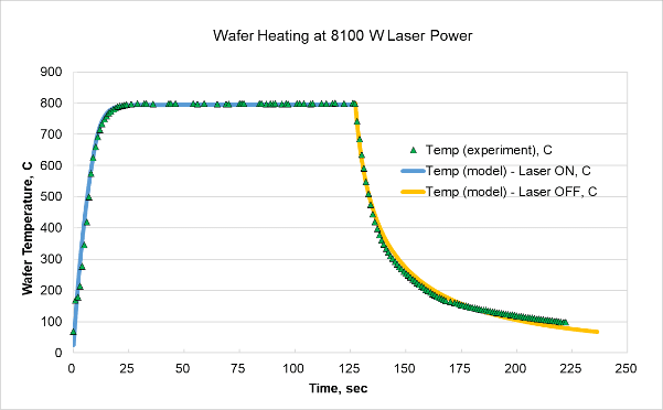
The experimental demonstration is shown in FIGURE 1. At full 11 kW power we heat the wafer to 800° C in less than 9 s while accurately controlling the temperature increase using a sensitive and fast pyrometer feedback control loop. Once 800°C is reached, a power requirement of only 8.1 kW laser power is sufficient to maintain the temperature. The experiment was repeated at various power and temperature settings, enabling us to develop a semi-empirical model incorporating known physical constants and thermodynamic formulae for radiative and convective processes along with fitting parameters. FIGURE 2 shows the excellent fit obtained between the 800°C wafer heating experiment and the model. Similarly close fits to the data gathered at other power levels and target temperature provide us with confidence to apply the model to predict performance on 300 mm wafers as well.
Click here to read the full article in Semiconductor Digest magazine.