“Data, data everywhere.. what am I to think?” This riff on the Rime of the Ancient Mariner may well be the lament of every engineer in the semiconductor industry who feels as if they are drowning in data. Fortunately, new tools are now available that combine visualizations and advanced analytics to allow them to quickly sort through data and find solutions.
The need for data analysis is worldwide, across every industry. According to a recent study by Spotfire, a business unit of Cloud Software Group, 30% of global organizations don’t have the right skills internally to analyze data, while the same amount are still struggling to understand which data is relevant and useful to them.
The survey, which questioned 1,200 IT leaders across the U.S, UK, France, and Germany, showed that for the majority of respondents (73%), data is firmly embedded throughout their business and is fully integrated into all decision-making. Almost a quarter (23%), however, feel data is still only being utilized somewhat effectively and they could be doing more with it.
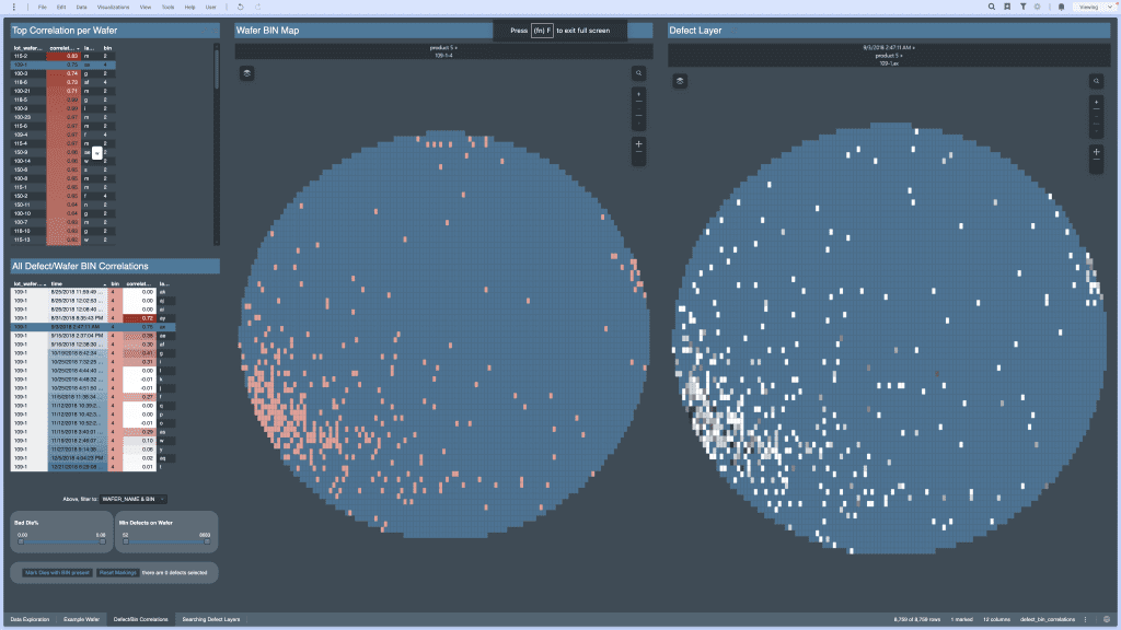
The same holds true in semiconductor manufacturing. Leading-edge semiconductor companies currently generate several TB of data per day but are only able to actively deal with a fraction of this data stream. “The industry is drowning in data. We’re talking about pressure, temperature, gas flows, facility, defects, metrology, electrical tests, functional tests, equipment maintenance, and parts and spares,” said Brad Hopper, VP for Vertical Markets at Spotfire. “It’s just a sea of information and with IoT, it’s just getting deeper and bigger every single day.”
There is a huge demand for systems to process data as rapidly as possible to facilitate quick diagnostic or wafer disposition decisions with minimum human intervention and avoid storing huge quantities of raw data. This requires comprehensive data analytics systems that span the entire IC manufacturing supply chain, from front-end wafer manufacturing to fully packaged systems to customer fulfillment.
Common examples of where data analytics are used include:
- Predictive Maintenance: By analyzing data from equipment sensors, manufacturers can predict when a machine is likely to fail and perform maintenance before a breakdown occurs.
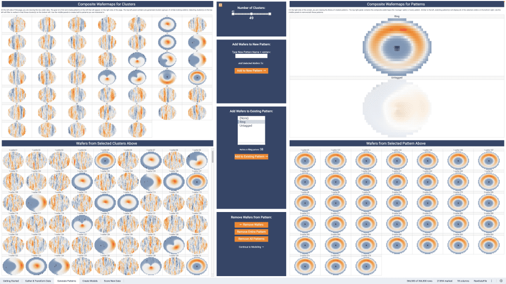
- Yield Optimization: Advanced analytics techniques, such as machine learning, can detect patterns and anomalies that human operators might miss, enabling manufacturers to make data-driven decisions to improve yield.
- Process Control: By analyzing data from sensors and production equipment, manufacturers can detect deviations from optimal conditions and make adjustments to maintain process stability.
- Defect Detection and Classification: Data analytics, combined with image processing and machine learning, can automate the detection and classification of defects. This automation reduces the reliance on manual inspection and increases the accuracy and speed of defect identification.
An elegant solution
To analyze data for these and other types of applications, semiconductor manufacturing companies have typically used a combination of what Spotfire’s Hopper calls “vertical” software – which includes yield management, MES and EDA software – and statistics software. Hopper said vertical software is powerful and highly tailored to specific use cases, but often very expensive and hard to use. At every company there are “only 10 guys who are experts and everyone says, ‘Hey Joe, can you help me do this thing with our yield management software?’” Hopper said.
Similarly, statistics software if very powerful, but understood by only a handful of experts. “The first question when you open it up is, ‘do you have a Weibull distribution or a Poisson distribution or a binomial distribution? Let’s get started,’” Hopper said. Companies typically have statisticians on staff – even Six Sigma Black Belts – that are power users of this kind of software, but their availability is limited. “Everybody else has statistics software, but they don’t really know how to use it,” Hopper said. “They go ask their statistician for help.”
The Spotfire solution provides an alternative to vertical software and statistics software. By combining visual data science with industry-specific advanced analytics, it allows engineers to come up with their own solutions instead of going off in search of a statistician. This means the most important people in the company are equipped with the tools they need. “We provide out-of-the-box advanced analytical calculations that you might find in a statistics tool, but we also have an open platform for our customers to deliver use-case specific advanced functionality for whatever that might be, whether it’s product reliability or process characterization or any of a long list of applications,” Hopper said. Spotfire can handle any kind of data – from defect images to parts and spares – and provide visual exploration of that data. “You can slice and dice it and make calculations,” Hopper said, “Or you can ‘mash-up’ heterogenous information which is often one of the biggest challenges.”

Click here to read the full article in the August/September issue of Semiconductor Digest.