By NICK KELLER and ZHUAN LIU, Onto Innovation, Milpitas, CA
Gate-all-around (GAA) transistors offer significant performance advantages at advanced nodes, but only at the cost of significant increases in process complexity. Complicated three-dimensional structures and shrinking critical dimensions make precise, accurate metrology in GAA manufacturing processes both more important and more challenging. Scatterometry-based optical critical dimension (OCD) metrology has become mainstream in the last several generations of semiconductor development, in part because of its ability to measure three dimensional shapes and subsurface/re-entrant features. The latest generation of OCD systems combines improvements in signal-to-noise ratios, signal fidelity and advanced machine learning capabilities that allow it to support the most challenging GAA process steps with repeatable measurements and production worthy throughput.
GAA vs planar and finFETs
The revolution in electronics that became the semiconductor industry was built on the discovery that the flow of electric current could be controlled by transistors fabricated from semiconductor materials, and the subsequent developments that found ways to continually decrease the size of those transistors. For most of its history, the industry has focused on planar transistor architectures in which a gate positioned over a channel controls the flow of current through the channel between a source and a drain. A voltage applied to the gate creates an electric field (FET – field effect transistor) that excludes or permits carriers in the channel thus turning the current on or off. The source, channel, and drain are coplanar, created at the surface of a semiconductor wafer, with the gate positioned over the channel (FIGURE 1). Increasing the computing power of an integrated circuit is essentially an exercise in reducing its aerial (X and Y) dimensions.

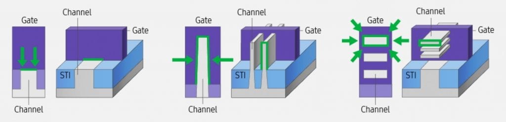
As nominal gate lengths (nodes) approached 20nm, planar devices encountered short channel effects, such as increasing leakage currents, that degraded their performance. To combat these effects manufacturers moved to finFETs, in which the channel has the shape of a fin, surrounded on three sides by the gate (Fig. 1). This increased the effective area of the gate in proximity to the channel. FinFET devices have allowed continuing increases in computing power through the current leading-edge nodes – around 5nm. (The node name no longer accurately reflects the gate length but is rather a convention to reflect successive generations on increasing device density and computing power.) Beyond this node, manufacturers have encountered limitations for finFETs and have had to consider other architectures. Several have chosen the gate-all-around (GAA) design in which, as the name suggests, the gate completely surrounds the channel (Fig. 1). GAA devices promise continuing improvement in performance but include three dimensional features that greatly increase the complexity of the manufacturing process.
Process control and optical metrology
Process control, ensuring that the process reliably creates functional devices with physical and electrical characteristics that fall within established process windows, is an essential part of every semiconductor manufacturing operation. Metrology, the science and practice of measuring process performance, provides the basis for process control. Just as manufacturing processes have evolved to create smaller, more complex devices, measurement technologies have had to change to monitor the new processes. Most image-based optical metrology became obsolete as critical dimensions (CD) decreased into the sub-micrometer range decades ago. The mainstay of the industry since that time has been scanning electron microscopy – specially designed for CD measurements (CD-SEM). CD-SEM is non-destructive and provides top-down, two-dimensional measurements. Cross sectional SEM (XSEM) can provide three-dimensional information, but at the cost of additional, destructive sample preparation. As device sizes have continued to decrease, dimensions have exceeded the resolution of SEM and manufacturers have adopted transmission electron microscopy (TEM). TEM can resolve individual atoms, but only at the cost of time-consuming, destructive sample preparation. It remains the gold-standard for accuracy and reference measurements, but its slow turnaround and low throughput are not well-suited to process control applications.
Although critical dimensions long ago passed beyond the resolution capability of optical imaging, other optical techniques can deliver fast, repeatable, non-destructive measurements. Optical critical dimension (OCD) measurements based on scatterometry derive shape, dimension and composition information from the scattering patterns observed in light that has interacted with the sample. It requires a regular array of similar features, but these are common in integrated circuits. The target may be an in-circuit feature, such as a line array, or a specially designed measurement target, typically located in the area between die on the wafer.
The simplest illustration of an OCD a measurement is the interference pattern created when light falls on a regularly spaced array of lines and spaces. The spacing of the interference fringes is a function of the wavelength of the light, the configuration of the optical path, and the spacing of the lines. Because the information is carried in the phase relationships of the light waves, the technique is not constrained by wavelength-related diffraction limits on image resolution. As manufactures moved beyond the 20nm node and adopted finFET architectures with critical three-dimensional features, scatterometry entered the mainstream of process control metrology.
Scatterometry for semiconductor manufacturing process control is based on ellipsometry. An ellipsometer measures the effects of reflection (or transmission) on polarized light. Ellipsometry has long been used in semiconductor metrology to characterize thin films in multilayer stacks. It is exquisitely sensitive and accurate, capable of measuring films as thin as a single atomic layer. Ellipsometers measure a material’s complex refractive index or dielectric tensor to determine fundamental physical properties. They can be used to characterize film thickness, composition, roughness, crystalline nature, doping concentration, electrical conductivity, and more.
Conventional ellipsometers look at polarized light reflected from the sample and compare it to the known polarization state of the incident light to measure the complex reflectance ratio, composed of two parameters, an amplitude component (ψ) and a phase shift difference (Δ). Spectroscopic ellipsometers use a broadband light source and measure these parameters as a function of wavelength. When used to measure thin, unpatterned films, the analysis typically assumes the sample is composed of a small number of discrete, well-defined layers that are optically homogeneous and isotropic. These assumptions are valid, and the two parameters, ψ and Δ, are sufficient, for most thin film applications.
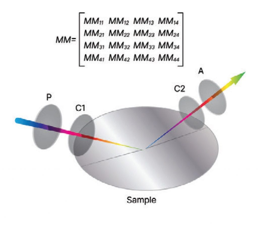
The assumptions are not valid for scatterometry measurements of complex three-dimensional features. Conventional spectroscopic ellipsometry measures only the amount of incident p-polarized (electric field parallel to the plane of incidence) light that is reflected as p-polarized light and the amount of incident s-polarized (electric filed perpendicular to the plane of incidence) light that is reflected as s-polarized light. However, there may also be cross polarized scattering, p to s and s to p. Mueller matrix spectroscopic ellipsometry (MMSE) captures a complete description of the polarized reflection, including cross-polarization and circular polarization, in a matrix of 16 elements at each wavelength. Cross polarization carries important information about characteristics such as symmetry, edge roughness and anisotropic optical properties. It is essential for characterizing 3D structures. The full Mueller matrix can be measured using a spectroscopic ellipsometer with dual rotating compensators (FIGURE 2), one between the polarizer and the sample and one between the sample and the analyzer.

The utility and value of full Mueller matrix ellipsometry varies with the application. In some cases, it is essential, such as the measurement of structural anisotropy like tilt and overlay shift. In other cases, it is not necessary, but still valuable, such measurements of complex structures where the additional information can help in parameter decorrelation. Finally, the additional information may be only potentially valuable but is essentially free, as when the dual compensators allow full Mueller matrix collection without using different analyzer angles.
Data analysis – RCWA and machine learning
OCD is an indirect measurement. No analytical solution exists to derive the desired physical or material properties directly from the measured parameters. Rather, the process relies on the development of models and their comparison to acquired data. The classic process relies on rigorous coupled wave analysis (RCWA) to generate a set of expected Mueller matrix elements based on theoretical interactions of light with a virtual model of the structure that includes shape, dimensions, material and optical properties, and more. Parameters of the model are varied, and the resulting matrix elements recorded. Regression analysis seeks to identify key features of the matrix element spectra that vary predictably and uniquely with the parameter of interest and can therefore serve as reliable proxies. The modeling process can be time-consuming, computationally intensive, and expensive. In use, actual measurement data are compared to the modeled data to infer the desired measurement value.
Recent developments in artificial intelligence (AI) and machine learning (ML) offer significant improvement in the cost and time to solution. Machine learning essentially automates the process. Given an appropriate dataset of measured MMSE spectra and reference values, machine learning can often find the salient spectral features and quantify their relationships to the parameters of interest without physical modeling or structured regression analysis. ML-based solutions are unlikely to completely replace model-based solutions. Rather, they will provide a complementary capability for situations where modeling is especially challenging. The ideal space for ML solutions will be situations where modeling costs are high because of the complexity of the structure, the key parameter of interest has dominating or unique sensitivity in the signal, and reference data is abundantly available.
GAA process
One design for GAA transistors incorporates multiple vertically stacked nanosheet channels passing through a single gate. The GAA process flow bears some similarity to finFET processes. The process begins with the creation of a superlattice, a stack of alternating, epitaxially deposited silicon and silicon germanium layers. Trenches etched through the lattice create fin-like structures, with each fin containing 3-4 silicon nanosheet layers that will become the transistor channels. The silicon layers alternate with SiGe layers that will eventually be replaced by gate materials. Dummy polysilicon gates are deposited across the nanosheet-fins and spacer material conformally deposited over all. Source and drain are etched either side of the gate, cutting through and exposing the ends of the Si channels. In a series of critical steps, the exposed SiGe between the ends of the Si channels is selectively etched to create cavities for the inner spacers and inner spacers are deposited in the cavities (FIGURE 3). These features are extremely small and yet their dimensions are critical for several reasons. The depth of the cavity/inner spacer determines the length of the gate, the inner spacer protects the subsequently deposited source and drain during layer release when the dummy gate is etched away and replaced with gate materials, and the spacer suppresses parasitic capacitance between the source/drain and gate.

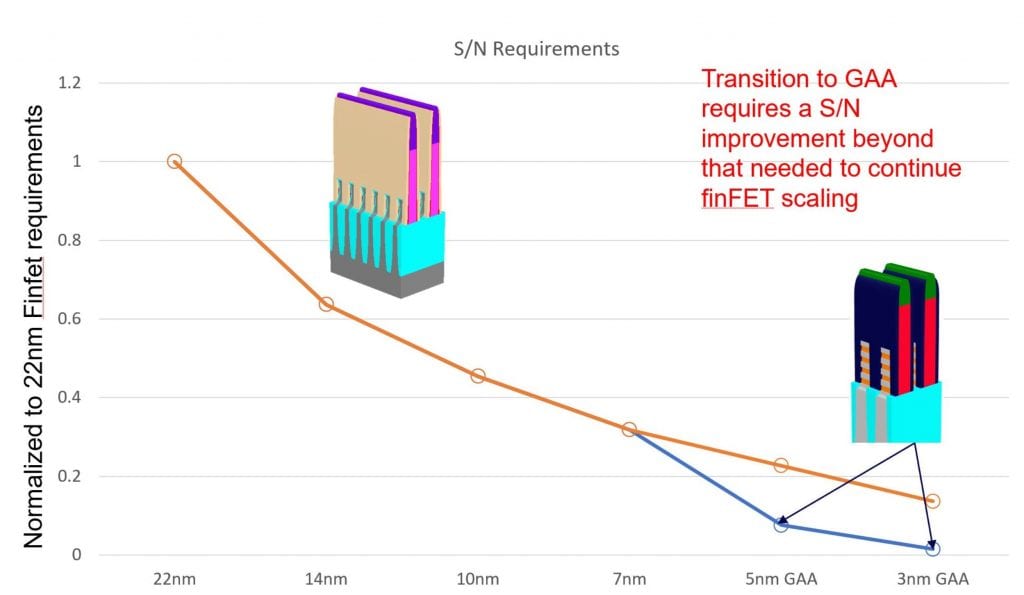
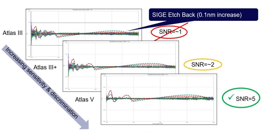
Each successive finFET node has required about a 30% improvement in the signal to noise ratio (S/N) in OCD systems (Figure 4). The transition to GAA architectures with exceptionally small, complex features like inner spacer cavities and inner spacers puts additional pressure on S/N. Still, OCD has the core capability needed for GAA processes. Onto Innovation has been developing OCD solutions for the GAA device with its Atlas OCD system. It was found that the earlier generation Atlas III system has a noise level close to the signal level for a 0.1nm increase in SiGe etch back, which limits the capability to measure the individual SiGe etch back. Improvements in the subsequently introduced Atlas III+ system provided a better signal for that measurement, and the recently introduced Atlas V system improves even more in signal to noise ratio, which provides the possibility to measure the individual dimensions of the SiGe etch back.
An overall (average) value for SiGe cavity etch is helpful, but what is really needed is a separate measurement for each spacer because the transistor will be defined by the “worst” nanosheet. The Atlas V metrology system, using the newly released AI-guided engine in the OCD solution software that includes both classical modeling and advanced machine learning capabilities, demonstrated individual inner spacer measurements with significant improvement in P/T (precision/tolerance) compared to average inner spacer measurements made with the Atlas III+ system (FIGURE 5).

Manufacturers are exploring other measurement technologies for some GAA process steps, most are X-ray-based. X-ray reflectivity (XRR) can measure the thin films in the initial superlattice, though this is an easy measurement for ellipsometry. High resolution X-ray diffraction (HRXRD) is useful for single crystal thin films. Onto Innovation has also done some work with critical dimension small-angle X-ray scattering (CD-SAXS), a scatterometry-like technique, but it is currently slow and expensive. X-ray photoelectron spectroscopy (XPS) is a surface analysis technique that can measure the composition, chemical state, and electronic state of elements in thin films.
Conclusion
GAA transistors are the most likely candidate to replace finFETs, putting more computing power in less space. They offer improved performance but require more complex processes to create smaller, three-dimensional structures. Controlling these processes requires improved metrology. OCD metrology has the fundamental capability. Current generation systems have demonstrated the ability to measure inner spacers, among the most challenging features. High-speed, non-destructive OCD metrology has the fundamental capability needed to support process control throughout the GAA process flow.
Reference
- https://www.overclock3d.net/news/misc_hardware/samsung_has_created_its_first_3nm_gaafet_prototypes_-_transistors_beyond_finfet/1