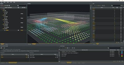
Anna Fontanelli, Monozukuri S.p.A. CEO and Founder, demonstrated MZ-GENIO, the first integrated IC/Packaging EDA tool, during the “Advanced 3D architecture and design methodology” session at DATE on Wednesday in Antwerp, Belgium.

During her session, Ms. Fontanelli showed how the MZ- GENIO™ holistic design environment spans the complete 3D design ecosystem. In doing so, its co-design platform enables a revolutionary approach to integrating with physical implementation tools in both IC and Package design spaces, as well as performing signal, power integrity and thermal analysis for physical-aware and simulation-aware system interconnect optimization.
She also demonstrated GENIO’s novel approach to creating never-before-seen levels of IC system integration that shortens the design cycle by two orders of magnitude, drives faster time-to-manufacturing, improves yields, and streamlines the entire IC eco-system to enable function-intensive IC-designs that will be the backbone for the most advanced next-generation integrated circuits.
“Shrinking transistors below a 1-nanometer node gets closer to the technology’s limit. To further scale IC-functionality means moving “off chip” to vertical IC integration. This, Ms. Fontanelli explains, is the most practical way – perhaps the only way – to increase design complexity, reduce time-to-market and lower per unit costs. Certainly, it’s more economically viable than extreme miniaturization,” she claims.
During her demonstration, Ms. Fontanelli offered the work that MZ Technologies is doing on Europe Horizon’s NibleAI Research Initiative as proof of GENIO’s capabilities.
For this project, the3D EDA tool supports technology-aware 3D physical architecture exploration across layers, a chiplet based floor planning approach enabling the use of multiple IP libraries to quickly explore different combinations of components and system configurations to find the most efficient component stack, and discover interconnection solution with the smallest footprint. Key is the fact that the tool remains agnostic to the different nature of the components and other tools used implementation and simulation, she explained.
GENIO™ features system architecture exploration, what-if analysis, 3D interconnect management, I/O planning and optimization, integrated within all existing EDA implementation platforms. It’s optimization algorithms tame the computational complexity of 3D designs. It supports all system architectures (2D, 2.5D, 3D configurations), all assembly styles (wire-bonding, flip-chip, and mixed) and all design flows (die-driven, package-driven, a mixture of top-down & bottom-up).