DAVE LAMMERS, Contributing Writer
The 2024 International Electron Devices Meeting (IEDM) was marked by the search for higher bandwidth, in multiple forms, including new memories, multi-chip packaging, and photonics.
Multiple presentations at IEDM discussed advances in ferroelectric devices which use a voltage to switch the polarization of a HfZO material rather than relying primarily on current. As such, Fe memories consume much less power, as much as 100x less. Also, ferroelectric devices are non-volatile, fast, and can be integrated in the metal layers of CMOS transistors.
At an evening imec forum, (ITF@IEDM), Jan Van Houdt, an imec fellow who manages the ferroelectric memory development group, said artificial intelligence “needs a memory which is non-volatile and low-power, and that’s FeRAMs.”
However, Van Houdt did not minimize the challenges. The HfZO material normally includes four crystalline phases, only one of which (the orthorhombic phase) is ferroelectric. “Maintaining that ferroelectric state is challenging,” he said.
Figuring out exactly where Fe-based memories fit in the memory hierarchy is also tricky. “There are a lot of papers at conferences, including IEDM, so the interest is definitely there. But it is not clear exactly what the application is,” he said.
Work to do at CEA-Leti
Laurent Grenouillet, who presented CEA-Leti’s work in ferroelectric memories at IEDM, also took a realistic attitude toward the memory hierarchy. Leti presented a 16-Kbit FeRAM, a 1T-1C array integrated in the M4-M5 layers of GlobalFoundries’ 22nm SOI CMOS base wafers. The Fe structures were built at CEA-Leti’s Grenoble fab.
FeRAMs can be fast (10 ns reads), with high endurance, and – “on paper” – very dense, while requiring minimal current. However, Grenouillet said “we still have work to do. How to improve the endurance of the devices — understanding the role of oxygen vacancies in films — is one challenge. He emphasized a Georgia Tech presentation on the use of an oxygen reservoir to extend the lifetime of the devices, as well as another IEDM presentation featured the use of tungsten-based electrodes to extend the remnant polarization.
“It looks simple, but there are so many things to understand,” he said, with film stack engineering, higher temperatures for crystallization, and other issues.
“We created a 16 kbit array in this first demonstration, but if we want to convince the industry, we need to design larger arrays with much more complex structures. We are thinking about 32 Mbits, and perhaps it will take more than a year to design and tape out. The research community is strong on this, and my hope is that we can help demonstrate products in the medium term,” he said.
TSMC creates BEOL-compatible memory
Chun Chieh Lu, R&D technical manager at TSMC, presented a ferroelectric memory combining an oxide channel with the smallest-reported Fe cell of 0.009 square microns. The endurance of the OS-FeFET was improved by re-engineering the interface (IL) layer and the HZO (hafnium zinc oxide) to minimize the oxygen vacancies, leading to “outstanding endurance.”
Lu said TSMC’s work achieved a small switching energy, fast write speed, and “non-volatile characteristics” suitable for “future low-power, high bandwidth, and high-capacity AI memory applications.”
“This work paves the way to realize BEOL-compatible memory with high density and low power consumption,” Lu said.
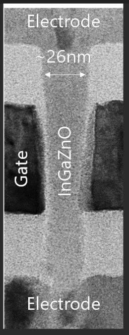
InGaZnO vertical channel transistors
A team of Kioxia and Nanya researchers developed an oxide-semiconductor vertical channel transistor DRAM (OCTRAM). Shosuke Fujii, an emerging memory researcher at Kioxia, presented a 4F2 architecture with the transistor on top of a high aspect ratio capacitor. The InGaZnO vertical channel transistors are manufacturable, with a 275-Mbit OCTRAM array “successfully fabricated, demonstrating the potential for future high-density, low-power DRAM technologies.”
These futuristic memory types absorbed much of the attention at the IEDM memory sessions, but orthogonal developments in chip stacking may be a more near-term solution to memory bandwidth challenges.
Stanford has put together a team to do a systematic study of the memory problems facing AI/HPC computing. Prof. Philip H.S. Wong observed that “it is fairly difficult to keep up with the memory needs of certain types of data access patterns, where optimally we might use different types of memory.”
While the industry sorts out the new memory types, Wong noted that 3D integration is rapidly shrinking the pin pitch of advanced chip stacking to below 1 μm. “These high-connection densities enable re-architecting the system to exploit potentially massive increases in bandwidth,” Wong said.
Hybrid bonding to sub 1-micron
During IEDM, Applied Materials organized an evening panel discussion on advanced packaging. AMD senior fellow Deepak Kulkarni said hybrid bonding is enabling “multi-tier stacking of chiplets.” By using relatively large panels, potentially more efficient stacking of heterogenous device types is possible, providing “clusters of chips to complete AI tasks.”
“Hybrid bonding in HBMs (high bandwidth memories) has proven it can lower the power consumption and flatten the (power) curve,” Kulkarni said.
Johanna Swan, director of package research at Intel, said “AI is all about managing power.” Hybrid bonding is moving toward sub-1-micron connections, though she said challenges remain in yields, reworkability, and moving from plastic to glass substrates.
Photonic links were much discussed at the 2024 IEDM, as the data center industry moves from photonics primarily for long links to connecting racks and processors within servers. The Applied Materials panelists called for photonics standards to enable co-packaged optics.
“The demand is there. We still have to figure out how to do it,” Swan said.