Researchers have reported a black phosphorus transistor that can be used as an alternative ultra-low power switch. A research team led by Professor Sungjae Cho in the KAIST Department of Physics developed a thickness-controlled black phosphorous tunnel field-effect transistor (TFET) that shows 10-times lower switching power consumption as well as 10,000-times lower standby power consumption than conventional complementary metal-oxide-semiconductor (CMOS) transistors.
Gigaphoton Unveils New Lasers for 2020
Gigaphoton Inc. (Head Office: Oyama, Tochigi; President & CEO: Katsumi Uranaka), a manufacturer of light sources used in semiconductor lithography, announced on February 21, 2020 that it will add two new models to its ArF and KrF product lineups in 2020. The ArF immersion “GT66A” and the KrF “G60K” light sources will bring the very latest technologies to semiconductor lithography manufacturing.
New Version of Si2 oaScript Expands IC Design Capabilities into the Cloud and AI
Design partitioning and multi-threaded parallel execution are key features of the updated scripting interface to OpenAccess, the industry’s most widely used IC design database. oaScript Version 4.0—developed by programming experts in the Silicon Integration Initiative oaScript Working Group—leverages the powerful enhancements available to OpenAccess in its most recent Data Model 6 upgrade.
Silvaco Appoints Howard Hideshima as Chief Financial Officer
Silvaco, Inc., a leading global provider of software, IP, and services to semiconductor companies for the design of ICs, flat panel displays, and electronic systems, today announced the appointment of Howard Hideshima as Chief Financial Officer (CFO).
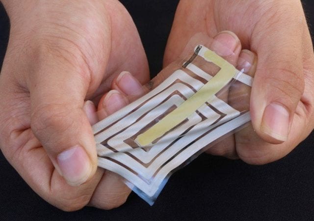
More Than Skin Deep: Skin-Inspired Electronics for Smart Healthcare at FLEX|MSTC 2020
As the body’s largest organ, skin is responsible for the transduction of a vast amount of information. This conformable, stretchable, self-healable and biodegradable material simultaneously collects signals from external stimuli, which translates into information such as pressure, pain and temperature.
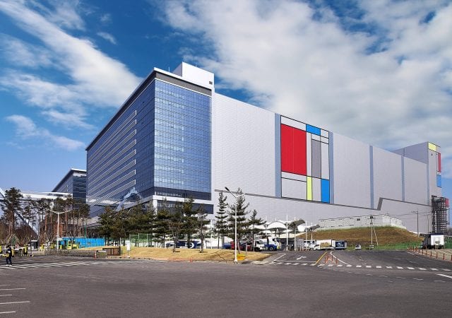
Samsung Electronics Begins Mass Production at New EUV Manufacturing Line
Samsung Electronics Co., Ltd., a world leader in advanced semiconductor technology, today announced that its new cutting-edge semiconductor fabrication line in Hwaseong, Korea, has begun mass production.
CEA-Leti’s Energy-Harvesting ICs Point the Way To Battery-Free Sensor Systems in Humans Or in Harsh Environments
In scientists’ quest for ambient-energy sources that can power sensor nodes in remote environments or difficult-to-reach settings where batteries are impractical, CEA-Leti takes a wide view. It is investigating harvesting systems ranging from micrometer-and-millimeter scale to centimeter scale or larger.
A Spookily Good Sensor
Scientists from the Research Center for Advanced Science and Technology (RCAST) at The University of Tokyo demonstrated a method for coupling a magnetic sphere with a sensor via the strange power of quantum entanglement. They showed that the existence of even a single magnetic excitation in the sphere could be detected with a one-shot measurement. This work represents a major advancement toward quantum systems that can interact with magnetic materials.
Questex’s Sensors Expo & Conference 2020 Adds New Features Aimed at Educating and Showcasing “What’s Next” for Rapidly Evolving Industry
Sensors Expo & Conference unveiled the widely anticipated 2020 Conference Program. Taking place June 22-24 at the McEnery Convention Center in San Jose, California, the 35th annual event will build upon its legacy of showcasing and educating on innovative sensor technology and dive deeper into the technologies, systems, and applications where sensors play a critical role – including the Internet of Things, Autonomous Technologies, and Embedded Systems.
STMicroelectronics and TSMC Collaborate to Accelerate Market Adoption of Gallium Nitride-Based Products
STMicroelectronics (NYSE:STM), a global semiconductor leader serving customers across the spectrum of electronics applications, and TSMC (TWSE:2330, NYSE: TSM), the world’s largest dedicated semiconductor foundry, are collaborating to accelerate the development of Gallium Nitride (GaN) process technology and the supply of both discrete and integrated GaN devices to market. Through this collaboration, ST’s innovative and strategic GaN products will be manufactured using TSMC’s leading GaN process technology.