ZEISS today introduced the ZEISS Crossbeam Laser — a new family of site-specific focused ion beam scanning electron microscope (FIB-SEM) solutions that accelerate package failure analysis and process optimization for advanced semiconductor packages. Integrating a femtosecond laser for speed, a gallium ion (Ga+) beam for accuracy, and SEM for nanoscale-resolution imaging, the ZEISS Crossbeam Laser family provides package engineers and failure analysts with the fastest cross-section solution at the highest imaging performance, while providing minimal sample damage.
SEMI Postpones SEMICON China, Suspends SEMICON Korea in Response to Coronavirus Outbreak
In accordance with government guidelines and to protect the health and safety of exhibitors and guests, SEMI announced Tuesday the postponement of SEMICON/FPD China 2020 and related events originally scheduled for March 18-20, 2020. SEMI China is actively working on a contingency plan for rescheduling of the event and will keep you informed as soon as a confirmed plan is in place.
Clock Tree Optimization Methodologies for Power and Latency Reduction
Widely used clock structures are described, with an emphasis on practical implementations of conventional clock tree structures along with H-Tree.
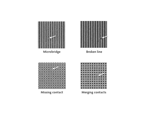
EUV Lithography: Sailing Along the Stochastic Cliffs
Stochastic printing failures are random, non-repeating, isolated defects such as microbridges, locally broken lines and missing or merging contacts.
EUV Lithography: Weighing the Options for Future Logic and Memory Applications
Imec takes a great leap forward in understanding and pushing the limits of extreme ultraviolet lithography – part I

Abating Potentially Dangerous Particles 2.5 µm and Smaller
Particles, especially fine particles, are very important because of their impact on human health.
NeoPhotonics Samples High Power Semiconductor Optical Amplifiers and Narrow Linewidth Lasers for Coherent Lidar Transceivers
NeoPhotonics Corporation (NYSE: NPTN), a leading designer and manufacturer of advanced hybrid photonic integrated circuit based modules and subsystems for bandwidth-intensive, high speed communications networks, today announced that it is sampling high power Semiconductor Optical Amplifiers (SOAs) and Narrow Linewidth (NLW) Distributed Feedback Lasers (DFB) lasers for long range automotive Lidar (“light detection and ranging”) applications.
ON Semiconductor to Explore Sale of Manufacturing Facility in Belgium
ON Semiconductor Corporation (Nasdaq: ON), driving energy efficient innovations, today announced it is exploring a sale of its manufacturing facility in Oudenaarde, Belgium. The company will begin searching for strategic partners that are willing to enter into a mutually beneficial arrangement that the company expects will facilitate an orderly transition of products from its Oudenaarde facility to other facilities within the ON Semiconductor network.
Next Generation of Mobile Devices Will Be Invisible
SEMI’s Nishita Rao caught up with Mike Wiemer, Ph.D., VP of Engineering, CTO and co-founder, Mojo Vision, to preview his February 25 keynote, The Art of the Possible, at FLEX|MEMS & Sensors Technical Congress (MSTC) 2020, February 24-27 at the DoubleTree by Hilton in San Jose, California.
SEMI-FlexTech Launches Six New Projects to Accelerate Flexible Hybrid Electronics Innovation
SEMI-FlexTech today announced the launch of six projects to accelerate sensor and sensor system innovations for new applications in industries including healthcare, automotive, industrial and defense. In collaboration with the U.S. Army Research Laboratory (ARL), FlexTech, a SEMI Strategic Association Partner, will provide more than $2.3 million in funding for the projects aimed at maturing the flexible-hybrid electronics (FHE) technology ecosystem