Leti, an institute of CEA-Tech, has developed a silicon nitride (Si3N4) 200mm platform for developing ultralow loss, high-power photonics in UV through mid-infrared wavelengths. Available in CEA-Leti’s SiN platform in a multi-project-wafer program, the breakthrough targets designers in integrated quantum optics, LiDAR, biosensing, and imaging whose projects require ultralow propagation losses and high-power handling capability.
Seoul Viosys and Seoul Semiconductor Develop a Single-Pixel RGB ‘Micro Clean LED’
Seoul Viosys Co., Ltd. and Seoul Semiconductor Co., Ltd.(KOSDAQ 046890), leading global innovators of LED and UV technologies, announced the development of their Micro Clean LED, a single-pixel RGB micro-LED technology that enables the design of 4K-resolution TVs with 42” to 220” displays. Introduced at the recent CES 2020, the world’s largest consumer electronics and technology exhibition, the Micro Clean LEDs are ready for mass production.
Surface Preparation for Low Temperature CVD Si Epitaxy Processing
Methods for producing the pristine and stable hydrogen-terminated single crystal silicon surfaces required to achieve the specifications for LT CVD epi silicon layers are investigated.
Picosun’s ALD Technology Helps to Fight Climate Change
Picosun’s Atomic Layer Deposition (ALD) thin film barrier coating technology offers a solution for eliminating the use of hazardous process gases, sulphur hexafluoride (SF6) and nitrogen trifluoride (NF3). By switching to Picosun’s ALD nanolaminate barrier technology it is possible to obtain unmatched barrier performance with extremely thin, pinhole-free films. This also eliminates the need to clean the deposition equipment after every few process runs.
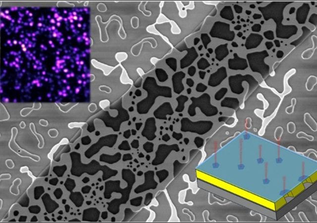
Coupled Quantum Dots May Offer a New Way to Store Quantum Information
Researchers at the National Institute of Standards and Technology (NIST) and their colleagues have for the first time created and imaged a novel pair of quantum dots — tiny islands of confined electric charge that act like interacting artificial atoms. Such “coupled” quantum dots could serve as a robust quantum bit, or qubit, the fundamental unit of information for a quantum computer. Moreover, the patterns of electric charge in the island can’t be fully explained by current models of quantum physics, offering an opportunity to investigate rich new physical phenomena in materials.
BJG Electronics Group Names Kent Smith as President
New York based BJG Electronics Group announced today that Kent Smith has joined the company as President, effective February 3, 2020. Most recently serving as Chief Commercial Officer for Integrated Supply Network, Smith brings to BJG a track record of successful leadership positions at electronics industry leaders. At Nu Horizons Electronics Corp., he served as President of the Americas and Asia-Pacific. Later, as Vice President of Sales at Arrow Electronics, he led a team that generated more than $4 billion in annual sales.
NRL Researchers’ Golden Touch Enhances Quantum Technology
Scientists at the U.S. Naval Research Laboratory discovered a new platform for quantum technologies by suspending two-dimensional (2-D) crystals over pores in a slab of gold.
Coronavirus Outbreak Can Drastically Impact the Technology Road Map for 2020, says GlobalData
The coronavirus outbreak is now entering a crucial phase with the WHO declaring it as a global health emergency. While the economic impact of the outbreak will be dependent on how long it ultimately lasts, its impact on technology markets across the world is already beginning to come to the fore, says GlobalData, a leading data and analytics company. Several technology companies, including Amazon, Microsoft and Apple have now imposed travel restrictions to and from China, whereas Google has altogether suspended its office operations in mainland China, Hong Kong and Taiwan.
AKHAN Semiconductor Issued Major Patent in United States
AKHAN Semiconductor, a technology company specializing in the fabrication and application of lab-grown, electronic-grade diamonds, announced today that it has been issued a patent by the United States Patent Office (USPTO). The patent covers AKHAN’s new and improved system and method for fabricating monolithically integrated diamond semiconductors.
CyberOptics Introduces New In-Line Particle Sensor as an Extension of the Industry-Leading Particle Sensing Technology at SPIE
CyberOptics Corporation (NASDAQ: CYBE), a global developer and manufacturer of high-precision 3D sensing technology solutions, will exhibit at SPIE Advanced Lithography from February 25-26, 2020 at the San Jose Convention Center in California, booth #308. During the show, the company will introduce its new In-Line Particle Sensor (IPS) with CyberSpectrum software for semiconductor tool set-up and equipment diagnostics.