Nepes (KOSDAQ: 033640), one of the top tier advanced packaging service providers, announces that it has initiated supply of high-reliability Fan-Out package service to a US based leading wireless chip maker. Fan-Out manufacturing is stabilized for mass production of the advanced package line recently acquired from Deca Technologies. “High Reliability Fan-out Package,” supplied by nepes, is a high-tech solution with more than 2 times BLR (Board Level Reliability) performance versus standard fan-out technologies by reducing physical stress on chips through sidewall protection structures.
Generation and Manipulation of Spin Currents for Advanced Electronic Devices
Graphene-based heterostructures of the van der Waals class could be used to design ultra-compact and low-energy electronic devices and magnetic memories. This is what a paper published in the latest issue of the Nature Materials journal suggests. The results have shown that it is possible to perform an efficient and tunable spin-charge conversion in these structures and, for the first time, even at room temperature.
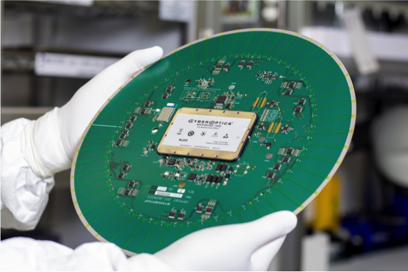
CyberOptics Unveils WaferSense Auto Resistance Sensor (ARS) at SEMICON Korea
CyberOptics® Corporation (NASDAQ: CYBE), a leading global developer and manufacturer of high-precision 3D sensing technology solutions, will exhibit at SEMICON Korea from February 5-7th, 2020 at the COEX in Seoul, booth #C236. During the show, the company will unveil and demonstrate its new WaferSense® Auto Resistance Sensor™ (ARS) with CyberSpectrum™ software for semiconductor tool set-up and diagnostics.
Colloidal Quantum Dot Laser Diodes Are Just Around the Corner
Researchers reach a critical milestone on the path to versatile colloidal quantum dot laser diodes by successfully demonstrating a quantum dot LED that also operates as an optically pumped laser.
Silicon Mobility Names Rainer Kallenbach as CEO
Silicon Mobility, the technology player powering control solutions for a cleaner, safer, and smarter mobility, is pleased to announce the appointment of former Robert Bosch GmbH executive Rainer Kallenbach as CEO of the company as of January 6, 2020. The current CEO Bruno Paucard will remain with the company as COO and on the Board of Directors.

Semiconductor Materials Growing to Nearly $50B Market in 2020 After Downturn
TECHCET—the electronic materials advisory services firm providing business and technology information— announced that global revenues for semiconductor manufacturing and packaging materials are expected to grow 5.7% year-over-year (YoY) in 2020 to US$49.5B, of which 65% represents semiconductor fab materials.
NY CREATES Begins Discussions on New Strategic Relationship With SEMI
The New York Center for Research, Economic Advancement, Technology, Engineering and Science (NY CREATES) today announced discussions to form a new Strategic Engagement with SEMI, the global industry association representing the electronics manufacturing and design supply chain. The announcement was made at the SEMI Industry Strategy Symposium, attended by several hundred C-Level semiconductor executives. Formed as a new and flexible industry interface in New York, NY CREATES is tasked with bridging academic, research, and industry innovation of the advanced electronics sector in New York.
Vitrex plc: Investment to Create a Joint-Venture for PEEK Manufacture in China
Victrex plc today announces the creation of a joint-venture between its subsidiary, Victrex Hong Kong Limited, and Yingkou Xingfu Chemical Company Limited, to build and operate a new PEEK polymer manufacturing facility in Liaoning, China, subject to certain performance conditions, including finalizing land purchase and permit applications. Victrex, which will be the majority partner and lead the joint-venture, will benefit by further differentiating and complementing its portfolio of PEEK and PAEK grades, in anticipation of a range of significant long-term growth opportunities across several end markets in China, as well as aligning with China’s ‘Made in China 2025’ initiative, where specifying domestically produced PEEK in certain applications is expected to gain momentum.
Cadence Expands Collaboration with Broadcom for 5nm and 7nm Designs
Cadence Design Systems, Inc. (Nasdaq: CDNS) today announced that it expanded its collaboration with Broadcom Inc. for the creation of semiconductor solutions targeting next-generation networking, broadband, enterprise storage, wireless and industrial applications. Building upon successful 7nm designs, Cadence and Broadcom are expanding the collaboration to include the creation of 5nm designs using Cadence® digital implementation solutions. With these Cadence solutions in place, Broadcom can further augment engineering productivity and improve silicon performance and power.
SEMI ISS 2020: Data Driven Innovation and Growth
The SEMI Industry Strategy Symposium (ISS) opened yesterday with the theme Data Driven Innovation and Growth. The annual three-day conference of C-level executives gives the year’s first comprehensive outlook of the global electronics manufacturing industry. For the nearly 300 attendees at ISS 2020, opening day highlighted market and technology opportunities and a reflection on the significant pricing and international trade challenges the semiconductor manufacturing supply chain faced in 2019.