Inphi Corporation (NYSE: IPHI), a leader in high-speed data movement interconnects, today announced that it has shipped more than 100,000 COLORZ® units, the industry’s first lowest power and most cost effective 100G Silicon Photonics PAM4 platform solution for 80km DWDM connectivity in a QSFP28 form factor. The demand for bandwidth, driven by streaming video, social networking, cloud computing and mobile e-commerce, is motivating network operators to deploy cloud applications closer to the end users.
Sublimation, Not Melting: Graphene Surprises Researchers Again
Physicists from the Moscow Institute of Physics and Technology and the Institute for High Pressure Physics of the Russian Academy of Sciences have used computer modeling to refine the melting curve of graphite that has been studied for over 100 years, with inconsistent findings. They also found that graphene “melting” is in fact sublimation. The results of the study came out in the journal Carbon.
MolecuLED Organic Color Conversion Technology Set to Revolutionize Large Screen TV and Horticulture Industries
StoreDot, a pioneer of ultra-fast charging (UFC) technology for electric vehicles, today announces the formation of a new, independent company to drive development of its unique MolecuLED wavelength conversion technology. The new business, named MolecuLED, will focus on the continued development of the technology in the TV and large display screen market, while exploring opportunities for transformative applications in industries such as horticulture and healthcare.
Bose and HERE Fuel AR Experience Innovation By Combining Location and Audio Technologies
HERE Technologies, a global leader in mapping and location platform services, today announced a collaboration with Bose Corporation to jointly enable their respective developer communities to deploy augmented reality (AR) location applications and services. This collaboration gives HERE developers access to the Bose AR platform and spatial-audio capabilities, and extends the HERE platform, positioning and mobile SDK location technologies to developers building audio AR applications and experiences.
AI Chip Company Syntiant Joins Qualcomm Extension Program
Syntiant, an AI chip company providing custom always-on voice solutions at the edge, today announced that it is now a member of the Qualcomm® Extension Program, offering OEMs and ODMs accelerated integration of its ultra-low-power neural network technology with Qualcomm® Bluetooth audio platforms and SOCs. With support from the Qualcomm Extension Program, Syntiant plans to deliver a touch-free, cloud- free, machine learning voice solution for always-on speech applications in battery-powered devices, such as Bluetooth-enabled earbuds and hearable devices.
Murata and Google Team to Develop World’s Smallest AI Module With Coral Intelligence
Murata Electronics Americas announced today that it has created the world’s smallest artificial intelligence (AI) module in partnership with Google – the Coral Accelerator Module. The custom designed module packages Google’s Edge TPU ASIC within a miniaturized footprint. The solution overcomes some of the most pressing challenges in implementing AI solutions by delivering superior noise suppression and simplifying printed circuit board design in a smaller footprint. Miniaturization is key as all board space must be optimized to achieve highly robust functionality in space constrained operations. The result of this collaboration is a solution that speeds up the algorithmic calculations required to execute AI.
Dirac And NXP Announce Collaboration To Equip The NXP i.MX 8M Family Of Chipsets With A Premium Digital Audio Platform
Swedish sound pioneer Dirac and NXP® Semiconductors today announced a collaboration to combine one of the world’s most powerful audio chipsets with a market-leading digital audio platform. By equipping the NXP i.MX 8M family of chipsets with Dirac’s digital audio platform, OEMs can enable their devices with maximized, immersive, and adaptive sound across their complete range of products. This announcement is being made at CES 2020 at Dirac Booth #18123.
NXP Debuts i.MX Applications Processor with Dedicated Neural Processing Unit for Advanced Machine Learning at the Edge
NXP Semiconductors N.V. (NASDAQ: NXPI) today expanded its industry-leading EdgeVerse portfolio with the i.MX 8M Plus application processor – the first i.MX family to integrate a dedicated Neural Processing Unit (NPU) for advanced machine learning inference at the industrial and IoT (Internet-of-Things) edge. The i.MX 8M Plus combines a high-performance NPU delivering 2.3 TOPS (Tera Operations Per Second) with a Quad-core Arm® Cortex-A53 sub-system running at up to 2GHz, an independent real-time sub-system with an 800MHz Cortex-M7, a high-performance 800 MHz audio DSP for voice and natural language processing, dual camera Image Signal Processors (ISP), and a 3D GPU for rich graphics rendering.
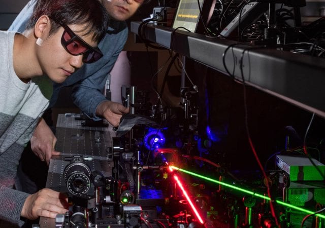
Laser Pulse Creates Frequency Doubling in Amorphous Dielectric Material
Researchers have demonstrated a new all-optical technique for creating robust second-order nonlinear effects in materials that don’t normally support them.
Renesas Electronics’ High-Efficiency Power Management IC Adopted in Google Coral AI Products
Renesas Electronics Corporation (TSE:6723), a premier supplier of advanced semiconductor solutions, today announced its ISL91301B Power Management IC (PMIC) is designed into the latest Google Coral products. They include the Mini PCIe Accelerator, M.2 Accelerator A+E Key, M.2 Accelerator B+M Key, and System-on-Module (SoM). Google Coral integrates seamlessly into processes at any scale, helping designers create a variety of local artificial intelligence (AI) solutions for several industries.