Weebit Nano (ASX: WBT), the next generation memory technology for the global semiconductor industry, and its development partner Leti, the French research institute recognised as a global leader in the field of micro-electronics, have filed three new patents for Weebit’s Silicon Oxide (SiOx) ReRAM
technology. The latest patents from Weebit and Leti use newly developed smart algorithms to increase the reliability and yield of ReRAM memory cells and enable scalable immune ReRAM process improvements. Two patents identify failure modes, in which optimised smart programming algorithms then improve the window margin and array yield. The third patent improves process flows, allowing increased stability at scaled memory cells in geometries of 40nm and below.
Weebit Nano and Leti File Three New Patents for Improved Yield and Reliability of Advanced ReRAM Products
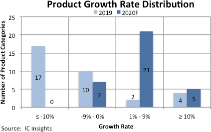
NAND Flash to Lead All Others As IC Market Growth Returns in 2020
IC Insights is in the process of revising its forecast and analysis of the IC industry and will present its new findings in The McClean Report 2020, which will be released in January 2020. Among the revisions is a complete update of forecast growth rates of the 33 main product categories classified by the World Semiconductor Trade Statistics organization (WSTS) through the year 2024. The top five categories for IC product growth are covered in this bulletin.
OneSpin Addresses the Challenges of RISC-V Verification at the Annual RISC-V Summit
OneSpin Solutions, provider of certified IC integrity verification solutions for building functionally correct, safe, secure, and trusted integrated circuits, will showcase its verification expertise of RISC-V processor cores at the upcoming RISC-V Summit being held December 10-12, 2019 at the San Jose Convention Center. OneSpin will host attendees at both its booth and a demo pod in the OpenHW pavilion at the RISC-V Summit, while the company’s experts will present two sessions on verifying RISC-V SoCs.
IEDM’s Monday is MRAM Day – Part 2
Samsung gives a second paper this session, detailing (2.5) A Novel Integration of STT-MRAM for On-chip Hybrid Memory by Utilizing Non-Volatility Modulation, with Jeong-Heon Park as lead author. “We demonstrate a novel way of integrating STT-MRAM for on-chip hybrid memory which exhibits either features of high-retention or high-speed implemented in separate zones in a single chip. For satisfying high temperature retention requirement, tailored MTJs are shown to support >10-year retention at 220℃.” MRAM switching protocols can be tuned for either high speed or high retention, so here we have a process which gives the option of both on the same die.
Diamonds In Your Devices: Powering the Next Generation of Energy Storage
Our use of battery-operated devices and appliances has been increasing steadily, bringing with it the need for safe, efficient, and high-performing power sources. To this end, a type of electrical energy storage device called the supercapacitor has recently begun to be considered as a feasible, and sometimes even better, alternative to conventional widely used energy-storage devices such as Li-ion batteries. Supercapacitors can charge and discharge much more rapidly than conventional batteries and also continue to do so for much longer. This makes them suitable for a range of applications such as regenerative braking in vehicles, wearable electronic devices, and so on.
Boréas Technologies’ New Chip-Scale Haptic IC Drives HD Touch in Smallest Electronics
Boréas Technologies, developer of ultra-low-power haptic technologies, today introduced the BOS1901CW, a Wafer Level Chip Scale (WLCSP) version of its flagship low-power piezoelectric driver integrated circuit (IC) for high-definition (HD) haptic feedback in mobile and wearable consumer products, including buttonless smartphones, smartwatches, game controllers and other battery-powered devices. Featuring WLCSP packaging, the BOS1901CW is just 2.1×2.2×0.6 mm and consumes just one-tenth the power of its nearest piezoelectric (piezo) competitor, making it small and low-power enough for the most resource-constrained devices.
Properties of Graphene Change Due to Water And Oxygen
The research team consisted of Professor Sunmin Ryu, Kwanghee Park, and Haneul Kang, affiliated with Department of Chemistry, POSTECH, discovered that the doping of two-dimensional materials with influx of charges from outside in the air is by an electrochemical reaction driven by the redox couples of water and oxygen molecules. Using real-time photoluminescence imaging, they observed the electrochemical redox reaction between tungsten disulfide and oxygen/water in the air. According to their study¸ the redox reaction can control the physical properties of two-dimensional materials which can be applied to bendable imaging element, high-speed transistor, next generation battery, ultralight material and other two-dimensional semiconductor applications.

Global Semiconductor Sales Increase 2.9 Percent Month-to-Month in October; Annual Sales Projected to Decrease 12.8 Percent in 2019
The Semiconductor Industry Association (SIA) today announced worldwide sales of semiconductors reached $36.6 billion for the month of October 2019, an increase of 2.9 percent from the previous month’s total of $35.6 billion, but down 13.1 percent compared to the October 2018 total of $42.1 billion.
Towards High Quality ZnO Quantum Dots Prospective for Biomedical Applications
Recently, scientists from the Institute of Physical Chemistry of the Polish Academy of Sciences (IPC PAS) and Warsaw University of Technology (WUT) in cooperation with the Interdisciplinary Research Institute of Grenoble (IRIG) used dynamic nuclear polarization (DNP)-enhanced solid state nuclear magnetic resonance (NMR) spectroscopy for detailed characterization of the organic-inorganic interfaces of ZnO QDs prepared by the traditional sol-gel process and the recently developed one-pot self-supporting organometallic (OSSOM) procedure.
SÜSS MicroTec and BRIDG Join Forces to Establish a Production-Level Applications Center in North America
SÜSS MicroTec, leading supplier of equipment and process solutions for the semiconductor industry, announced today a far-reaching collaboration agreement with BRIDG, a not-for-profit, public-private partnership focused on production process technologies, advanced system integration, and 200mm microelectronics fabrication advancing next-generation nanoscale technology. This partnership puts an unprecedented array of SUSS MicroTec equipment and fabrication technologies at the doorstep of its North American customer base, readily accessible for demonstrations and evaluations.