By David W. Price, Douglas G. Sutherland, Jay Rathert, John McCormack and Barry Saville
Author’s Note: The Process Watch series explores key concepts about process control—defect inspection, metrology and data analytics—for the semiconductor industry. This article is the third in a series on process control strategies for automotive semiconductor devices. For this article, we are pleased to include insights from our colleagues at KLA-Tencor, John McCormack and Barry Saville.
Semiconductors continue to grow in importance in the automotive supply chain, requiring IC manufacturers to adapt their processes to produce chips that meet automotive quality standards. The first article in this series1 focused on the fact that the same types of IC manufacturing defects that cause yield loss also cause poor chip reliability and can lead to premature failures in the field. To achieve the high reliability required in automotive ICs, additional effort must be taken to ensure that sources of defects are eliminated in the manufacturing process. The second article in this series2 outlined strategies, such as frequent tool monitoring and a continuous improvement program, that reduce the number of defects added at each step in the IC manufacturing process. This article explores how to drive tool monitoring to a higher level of performance in order to help automotive IC manufacturers achieve chip failure rates below the parts per billion level.
As a reminder, tool monitoring is the established best practice for isolating the source of random defectivity contributed by the fab’s process tools. During tool monitoring, a bare wafer is inspected to establish its baseline defectivity, run through a specific process tool (or chamber), and then inspected again. Any defects that were added to the wafer must have come from that specific process tool. This method can reveal the cleanest “golden” tools in the fab, as well as the “dog” tools that contribute the most defects and require corrective action. With plots of historical defect data from the process tools, goals and milestones for continuous improvement can be implemented.
When semiconductor fabs design their tool monitoring strategy, they must decide on the minimum size of defects that they want to detect and monitor. If historical test results have shown that smaller defects do not impact yield, then fabs will run their inspection tools at a lower sensitivity so that they no longer detect these smaller defects. By doing this, they can focus only on the larger yield-killer defects, avoiding distraction from the smaller “nuisance” defects. This approach works for a consumer fab that is only trying to optimize yield, but what about the automotive fab? Recall that yield and reliability issues are caused by the same defects types – yield and reliability defects differ only in their size and/or where they land on the device pattern.2 Therefore, a tool monitoring strategy that leaves the fab blind to smaller defects may be missing the very defects that will be responsible for future reliability issues.
Moreover, it’s important to understand that defects that seem small and inconsequential at one process layer may have a dramatic impact later in the process flow – their impact can be exacerbated by the subsequent process steps. The two SEM images in figure 1 were taken at exactly the same location on the same wafer, but at different steps of the manufacturing process. The image on the left shows a single, small defect that was found on the wafer after a deposition layer. This defect was previously thought to be a nuisance defect with no negative effect on the die pattern or chip performance. The image on the right shows that same deposition defect after metal 1 pattern formation. The presumed nuisance defect has altered the quality of the metal line printed several process steps later. This chip might pass electrical wafer sort, but this type of metal deformity could easily become a reliability issue in the field when activated by automotive environmental stressors.

Figure 1. The left image shows small particle created at a deposition layer. The right image shows the exact same location on the wafer after the metal 1 pattern formation. The metal line defect was caused by the small particle at the prior deposition layer. This type of deformity in the metal line could easily become a reliability issue in the field.
So how does an automotive IC fab determine the smallest defect size that will pose a reliability risk? To start, it is important to understand the impact of different defect sizes on reliability. Consider, for example, the different magnitudes of a line open defect shown in figure 2. A chip that has a pattern structure with a full line open will likely fail at electrical wafer sort and thus does not pose any reliability risk. A chip with a 50% line open – a line that is pinched or otherwise restricted to ~50% of its cross-sectional area – will likely pass electrical wafer sort but poses a significant reliability risk in the field. If this chip is used in a car, environmental conditions such as heat, humidity and vibrations, can cause degradation of this defect to a full line open, resulting in chip failure.

Figure 2. The image on the left shows a full line open, while the right image shows a ~50% line open. The chip on the left will fail at sort (assuming there is no redundancy). The chip on the right may pass electrical wafer sort but is a reliability risk in the field.
As a next step, it is important to understand how different size defects affect a chip’s pattern integrity. More specifically, what is the smallest defect that will result in a line open? What is the smallest defect that will result in a 50% line open?
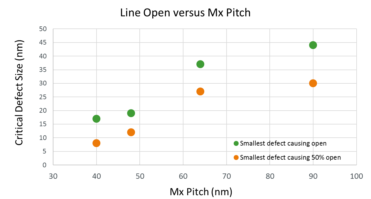
Figure 3 shows the results of a Monte Carlo simulation that models the impact of different size defects introduced at a BEOL film deposition step. Minimum defect size is plotted on the vertical axis against varying metal layer pitch dimensions. This data corresponds to the metal 1 spacing for the 7nm, 10nm, 14nm and 28nm design nodes, respectively.
The green data points correspond to the smallest defects that will cause a full line open and the orange data points correspond to the smallest defects that will produce a 50% line open (i.e., a potential reliability failure). In each case the smallest defect that will cause a potential reliability failure is 50-75% of the smallest defect that will cause a full line open.

Figure 3. The green data points show the minimum defect size required to cause a full line open at the minimum metal pitch. The orange data points show the minimum defect size needed to cause a 50% line open. The x-axis is the metal 1 spacing for the 7nm (far left data point), 10nm, 14nm and 28nm (far right data point) design nodes.
These modeling results imply that to control for, and reduce, the number of reliability defects present in the process, fabs need to capture smaller defects. Therefore, they require higher sensitivity inspections than what is required for yield optimization. In general, detection of reliability defects requires an inspection sensitivity that is one node ahead of the current design node plan for yield alone. Simply put, a fab’s previous standards for reducing defectivity to optimize yield will not be sufficient to optimize reliability.
Increasing the sensitivities of the tool monitoring inspection recipes, or in some cases, using a more capable inspection system, will find smaller defects and possibly reveal previously hidden signatures of defectivity, as in Figure 4 below. While these signatures may have had a tolerable impact on yield in a consumer fab, they represent an unacceptable risk to reliability for automotive fabs pursuing continuous improvement and Zero Defect standards.

Figure 4: Hidden defect signatures that may impact reliability are often revealed with appropriate tool monitoring sensitivity. Zero Defect standards require corrective action on the process tool contributing these defects.
There are several important unpatterned wafer defect inspection factors for a fab to consider when creating a strategy to improve tool monitoring inspection sensitivity to find the small, reliability-related defects contributed by process tools. First, it is important to recognize that in a mature fab where yields are already high, there is rarely a single process layer or module that will be the “silver bullet” to reducing defectivity adequately to meet reliability improvement goals. Rather, it is sum of small gains across many layers that produce the desired gains in reliability. Because yield and the associated reliability improvements are cumulative across layers, reliability gains achieved through process tool monitoring using unpatterned wafer inspection are best demonstrated using a multi-layer regression model:
Yield = fYs+fSFS1+fSFS2+ fSFS3+ ….. fSFSN + error
- Ys = systematic yield loss (not particles related)
- SFSx = cumulative Sursfcan unpatterned wafer inspection detected particles for many layers
- Error = Yield loss mechanisms not detected by Surfscan
This implies that reliability improvements require a fab’s commitment to continuous improvement in defectivity levels across all processes and process modules.
Second, the fab should consider the quality of the bare wafer used for process tool monitoring. Recycling bare wafers increases the surface roughness with each cycle, an attribute known as haze. This haze level is fundamentally noise that affects the inspection system’s ability to differentiate the signal of smaller defects. Variability in haze across the population of test wafers acts as a limit to overall inspection recipe capability, requiring normalization, calibration and haze limits to reduce the impact of this noise source on defect sensitivity.
Next, the fab should ensure that the monitor step closely mimics the process that a production, patterned wafer follows. Small time-saving deviations in the monitor wafer flow to short cut the process may inadvertently skip the causal mechanism of defectivity. Furthermore, an over-reliance on mechanical handling checks alone bypasses the process completely and misses the critical contribution the process plays in particle generation.
When increasing the inspection recipe sensitivity, the fab must co-optimize both the “pre” and “post” inspection together. Often cycling the bare wafer through a process step can “decorate” small pre-existing defects on the wafer that were initially below the detection threshold. Once decorated, the defects now appear bigger and are more easily detected. In an unoptimized “post” inspection, these decorated defects can look like “adders,” leading to a false alarm and inadvertent process tool down time. Optimizing the inspections together maximizes the sensitivity and increases the confidence in the excursion alarms while avoiding time-consuming false alarms.
Lastly, it is important to review and classify the defects found during unpatterned inspection to correlate their relevance to the defects found at the equivalent patterned wafer process step. Only then can the fab be confident that the source of the defects has been isolated and appropriate corrective action has been taken.
To meet the high reliability demands of the automotive industry, IC manufacturers will need to go beyond simply monitoring and controlling the number of yield limiting defects on the wafer. They will need to improve the sensitivity of their tool monitoring inspections to one node smaller than what would historically be considered relevant. Only with this extra sensitivity can they detect and eliminate defects that would otherwise escape the fab and cause premature reliability failures. Additionally, when implementing a tool monitoring strategy, fabs need to carefully consider multiple factors, such as monitor wafer recycling, pre and post inspection sensitivity and the importance of a fab-wide continuous improvement program. With so much riding on automotive semiconductor reliability, increased sensitivity to smaller defects is an essential part of an optimal Zero Defect continuous improvement program.
About the Authors:
Dr. David W. Price and Jay Rathert are Senior Directors at KLA-Tencor Corp. Dr. Douglas Sutherland is a Principal Scientist at KLA-Tencor Corp. Over the last 15 years, they have worked directly with over 50 semiconductor IC manufacturers to help them optimize their overall process control strategy for a variety of specific markets, including implementation of strategies for automotive reliability, legacy fab cost and risk optimization, and advanced design rule time-to-market. The Process Watch series of articles attempts to summarize some of the universal lessons they have observed through these engagements.
John McCormack is a Senior Director at KLA-Tencor. Barry Saville is Consulting Engineer at KLA-Tencor. John and Barry both have over 25 years of experience in yield improvement and defectivity reduction, working with many IC manufacturers around the world.
References:
- Price, Sutherland and Rathert, “Process Watch: The (Automotive) Problem With Semiconductors,” Solid State Technology, January 2018.
- Price, Sutherland and Rathert, “Process Watch: Baseline Yield Predicts Baseline Reliability,” Solid State Technology, March 2018.