ZSOLT TOKEI, imec fellow, and program director of nano-interconnects at imec
In 1997, the introduction of Cu dual-damascene integration schemes in the back-end-of-line (BEOL) of logic and memory chips marked an inflection point in semiconductor history. Chip makers moved away from subtractive Al patterning to wet processes like Cu electroplating and chemical mechanical polishing (CMP). This radical transition was needed to cope with an increasing RC delay in Al-based interconnects, the result of an increasing resistance-capacitance (RC) product. Being cost-effective and applicable to multiple layers of the BEOL stack, Cu dual-damascene was set to enable many subsequent generations of logic and memory technologies.
But in a few years from now, the metal pitches within the most critical BEOL layers will drop below 20nm. When that happens, Cu dual-damascene, in turn, will run out of steam. As shrinking metal line dimensions approach Cu’s electron mean free path, the RC delay will increase dramatically. In addition, Cu metallization requires a barrier, a liner and a cap layer to ensure good reliability and prevent Cu from out-diffusing into the dielectric. But these extra layers start to consume a large share of the total available line width, meaning that the precious conductive area cannot be fully utilized by the interconnect metal itself. These issues force the chip industry to investigate alternative metallization schemes with better figures of merit at tight metal pitches.
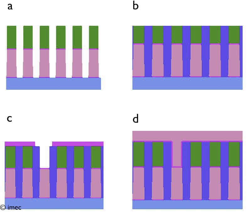
After filing an initial patent in 2017, imec presented a new metallization concept to the semiconductor community in 2020 and named it ‘semi-damascene’ [1]. Just like the Al-based metallization, semi-damascene integration starts with the direct patterning (or subtractive metallization) of the first local interconnect metal layer, hence requiring a patternable metal such as W, Mo, Ru, etc. (FIGURE 1). The via that connects with the next interconnect layer is then patterned in a single-damascene fashion: a hole etched into the dielectric is filled with metal and overfilled – meaning that the metal deposition continues until a layer of metal is formed over the dielectric. This metal is layer is subsequently masked and etched to form the second interconnect layer, with lines orthogonal to the first layer.

The value proposition of semi-damascene is promising. It can be regarded as a two-layer metallization module potentially expandable to multiple layers – making it cost effective. The subtractive etch allows for higher metal line aspect ratios (ARs) than conventional Cu interconnects, improving the resistance. As for the dielectric, the metal lines can potentially be combined with airgaps instead of low-k dielectric gap fill. Airgaps offer a lower dielectric constant, leading to smaller intra-level capacitance. Besides being RC efficient, semi-damascene also eliminates the use of metal CMP, simplifying the process flow and resulting in improved line height control. The use of refractory metals also presents benefits. They have the promise to be used without barrier layer, hence providing low via and line resistance. They are also more resistant to electromigration and overall offer lower resistance than Cu at reduced dimensions.
The industry’s response: a promising but disruptive technology
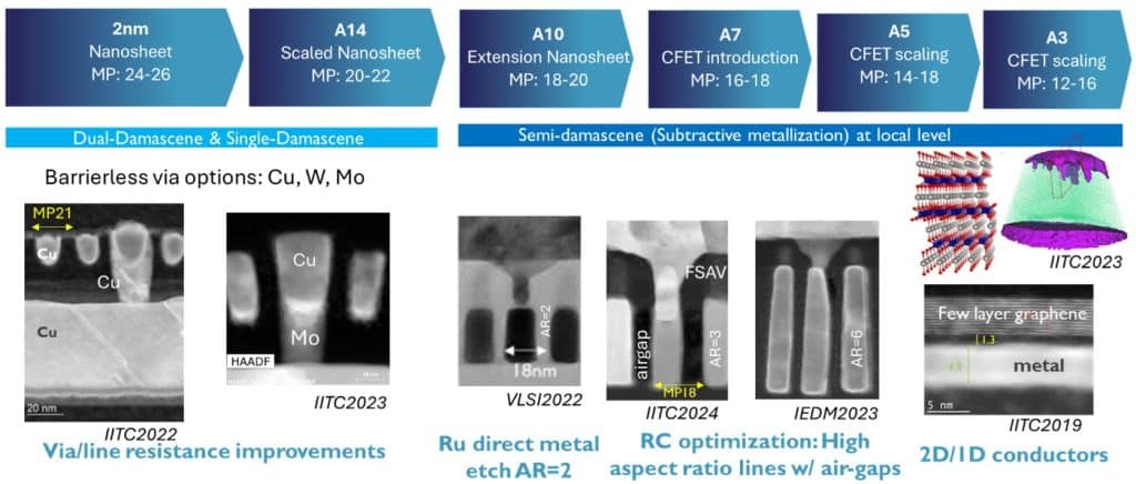
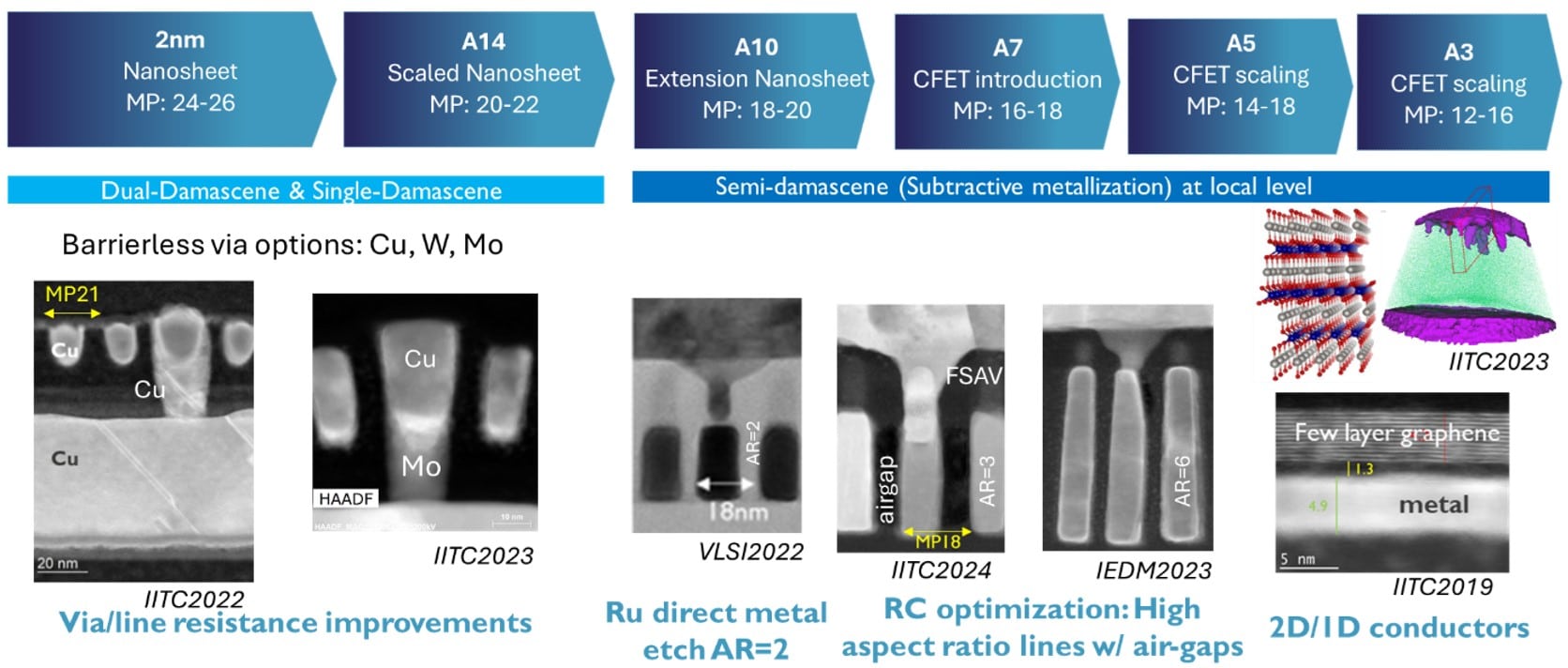
Since imec introduced semi-damascene integration, multiple organizations started to research similar new schemes, and steady progress has been made through simulations and experiments [2-5]. Today, the very first step of the scheme, i.e., the subtractive etch of the first metal layer, has been successfully demonstrated and reported at conferences by multiple organizations. Experiments have clearly shown that replacing Cu with subtractively etched Ru in the first local interconnect layer can already provide a much-wanted benefit, even at a modest line AR ~2. For subsequent generations the AR can be increased to 3 or 6 and then combine into multiple local metal layers. R&D evidence is growing that semi-damascene is indeed a valid option, offering an interconnect scaling path.
At the same time, there are question marks. Industry is currently considering moving the first generation of semi-damascene into development, the phase before actual production. As with any new technology, industry does not proceed overnight. Semi-damascene integration disrupts the conventional technology for fabricating the BEOL. It requires new tools and materials, and perhaps some of the defect mechanisms are not captured in the research phase. Such investments are of interest only if the technology can span several technology generations. While the first step with only one metal layer is adequately documented, the implementation of a two-layer and even multi-layer integration scheme – where the capabilities and benefits of semi-damascene can be fully exploited – is however less discussed. That’s why imec encourages the R&D community to open the discussion, help filling the remaining ‘gaps’ and share insights on multilayer integration at interconnect technology conferences.
The imec interconnect roadmap: introducing 5 generations of semi-damascene
Imec proposes to gradually introduce subsequent generations of semi-damascene. Insertion of the first generation is envisioned for the imec A10 or A7 logic technology node, where the metal pitch of the most critical interconnects becomes as tight as 18nm (FIGURE 2). At that point in time, GAA nanosheet integration is expected to be mainstream and CFETs will not yet be in place. Introducing semi-damascene will therefore be the only major change that chip makers will have to cope with.

Imec proposes to introduce subtractively etched Ru in M0, the first local metal layer that follows the middle of line (MOL). This first generation will come with a metal line AR 2, which is slightly higher than today’s typical Cu line AR (~1.6). In combination with the favourable behaviour of barrier-less Ru at tight metal pitches, this approach will already give a resistance and reliability benefit over Cu.
Read the full article in the October issue of Semiconductor Digest.
