The Shenzhen Institute of Advanced Technology (SIAT) of the Chinese Academy of Sciences collaborated with Nanyang Technological University (NTU) in Singapore to develop a mass production technology for high-quality semiconductor silicon and germanium fibers. This technology successfully transforms traditionally brittle semiconductors like silicon and germanium into flexible fibers, demonstrating innovative applications in flexible electronics through photoelectric fiber pn junctions.
The results were recently published in the journal Nature.
The flexible and stable “hair” sensors can be used independently or woven into fabric, turning passive clothing into functional “smart” wear. These fibers have broad application prospects in future intelligent wearables, the metaverse, artificial intelligence, extreme environment sensors, brain-computer interfaces, and other fields.
As an emerging form of inorganic semiconductor materials, one-dimensional fibers have unique advantages of fineness and softness. They offer new possibilities for the seamless integration of flexible electronic devices with daily clothing, creating non-intrusive links between technology and daily life.
However, rapid and large-scale production of high-quality semiconductor fibers has been a significant challenge for the scientific community. The research team drew inspiration from traditional optical fiber preparation and thermal drawing processes, extending the single material fiber thermal pulling method to the material preparation process. By addressing issues of stress mismatch and fluid instability from the perspectives of solid mechanics and fluid mechanics, they successfully achieved a production strategy for silicon/germanium semiconductor fibers, producing several meters to dozens of meters per minute.
Further, using a convergent thermal drawing method, the team-built interfaces between insulators, conductors, and semiconductors within a single hair-thin fiber.
“This method completes device assembly and encapsulation simultaneously”, said Prof. CHEN Ming, one of the corresponding authors from SIAT, “creating photoelectric fiber detectors that perform excellently under extreme conditions, like three kilometers underwater.”

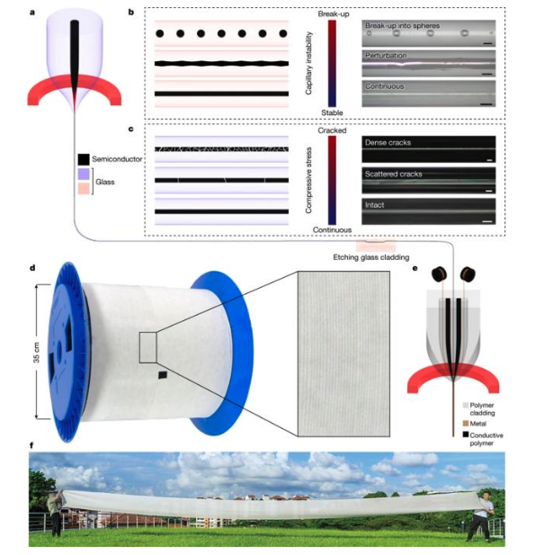
f) Functional fabric: Enabled by the resulting optoelectronic fibers. Credit: CHEN Ming