The way in which logic and memory technology is likely to evolve over the next six years was provided at imec’s recent International Technology Forum in Leuven, Belgium. An Steegan, senior vice president process technology at imec, said that FinFETs will likely become the logic technology of choice for the upcoming generations, with high mobility channels coming into play for the 7 and 5nm generation (2017 and 2019). In DRAM, the MIM capacitor will give way to the SST-MRAM. In NAND flash, 3D SONOS is expected to dominate for several generations; the outlook for RRAM remains cloudy.
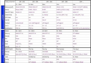
As shown in the Table, the 14nm node (which imec calls the “N” node”) is in development today, heading toward early production in 2013/2014. That will be followed by the N10 node in production at the end of 2015 and beginning of 2016. Then N7 and N5 will follow in 2017 and 2019.

The most notable evolution in the logic roadmap is that of device architecture, where planar devices are being replaced by fully depleted devices. There are two main flavors of fully depleted devices: fully depleted SOI (FDSOI) and finFETs. Imec sees FDSOI as an option for 14nm, which is “actually a speed push option from 20nm,” Steegen said. “What’s happening is that in the 14-16 generation, speed push knobs are implemented on the technology roadmaps to get the extra performance boost for that node.” That’s partly driven by the readiness (or really unreadiness) of EUV. “Scaling is not necessarily the .7X one dimensional scaling that you expect node to node,” Steegen said. That’s why, in the 16-14nm generation, planar devices are being replaced by a higher performing fully depleted device. “When you push this to 10 and 7nm that we believe that the finFETs are going to have a long lasting life,” she added, which means that we will see finFETs on the roadmap for at least three generations.
The two main advantage of fully depleted SOI versus planar: 1) area footprint. You always get more performance from a trigate device since you actually use that third dimension. 2) Power/performance benefits.
Steegen said imec is now mainly focused on assessing processes for 7nm and trying to figure out when the ultimate finFET scaling limit will be hit. At that point, expect to see what imec calls “local SOI,” which is a slight undercut of the bulk silicon fin to provide better isolation in the well. A more extreme version gate all-around device, which could be based on silicon nanowires.
To boost performance in the past, external source/drain stressors were used to increase electron and hole mobility in the device. The problem moving forward, in the N10 and N7 generations, is that there’s no space to do that. Instead, expect to see replacement of the silicon channel with a high mobility material. “When you look at what material that could be, germanium is a good candidate to push hole mobility, so the PFET. And III-V, InGaAs, is a good material for NFET devices to push the electron hole mobility,” Steegen explained.
As far as standalone memory (vs embedded memory) goes, STTRAM is now being pushed forward to basically replace the MIMCAP on the DRAM roadmap. That’s because it’s very challenging to get an EOT of 0.3 (see table) and maintain acceptable leakage of the MIM capacitor.
For NAND flash, Steegen said the two-dimensional hybrid floating gate integration flow is definitely being pushed to a 15 and 13nm half pitch. “Scaling is one challenge you’re going to encounter here. The other one is the charge you can trap on the floating gate itself. It becomes so discrete there’s hardly any charge left. The variability you’re going to have on the hybrid floating gate concept is likely getting too big. That is why 3D SONOS is definitely getting it’s way in on the NAND flash replacement roadmap and also we forecast that to have quite a long lifetime: two or three generations,” she said.
Steegen said the outlook for RRAM was cloudy. It could be the eventual successor to 3D SONOS, but “if you want to replace 3D SONOS, you’re getting to need 3D RRAM because you’re going to use the same 3D configuration. Also, for NAND flash replacement, you always need that select element to make sure you only select that one cell you want to turn on. How to integrate the selector with the RRAM element in a 3D configuration is going to be the trick of how RRAM can enter this NAND flash roadmap at the end,” she said.


