
The U.S. Department of Defense has announced that the Southwest Advanced Prototyping (SWAP) Hub based at Arizona State University (ASU) has been awarded $5.9M in funding through the CHIPS and Science Act for the new Spaceborne Low Energy AI Computing (SLEAC). The project, hosted by the SWAP Hub and led by ASU, is aimed at extending the power of artificial intelligence (AI) to satellites orbiting our planet.
Headquartered in Arizona, the SWAP Hub is part of the CHIPS and Science Act-funded Microelectronics Commons, a network of regional technology hubs. It connects the Southwest – the fastest-growing and largest semiconductor cluster in the United States, with more than $100 billion in private investment – to a growing network of defense and electronics partners across the country.
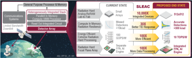
Advancing the performance of satellites through AI have the potential to unlock advances that will yield a major advantage for national defense. Computer hardware designed for spacecraft undergoes a manufacturing process called radiation hardening. It enables the equipment to survive exposure to harsh radiation levels in orbit, but it also compromises performance compared to state-of-the-art computing on Earth. If it were possible to directly integrate a highly efficient, radiation hard AI chip with focal plane array image sensors used in space, satellites could track objects that are too faint or too fast to be detected by current systems.
Energy efficiency is critical for achieving high performance in power-constrained systems like satellites. SLEAC aims to significantly surpass current state-of-the-art energy efficiencies, which are a few tera operations per second per watt (TOPS/W). This requires progressing beyond conventional digital processing architectures and using analog in-memory computing, or AIMC. Like a neuron that computes at each synapse in the brain, AIMC uses new analog memories to perform multiplication at each memory element.
“This goal has proven challenging because the standard memory technologies integrated into modern complementary metal-oxide semiconductor (CMOS) processes are charge-based and therefore highly sensitive to radiation,” says Matthew Marinella, the SLEAC project lead and an associate professor of electrical engineering at Arizona State University. “Radiation is particularly problematic for analog memory intensive AI architectures, such as AIMC.”
Marinella says the SLEAC project will overcome this challenge by using radiation hard metal oxide-based analog-optimized resistive memory (ReRAM) arrays integrated with foundry-supplied CMOS to create an AIMC prototype processor capable of more than 10 TOPS/W in extreme environments. This would be several times more efficient than modern unhardened systems and over 100 times more efficient than the current state of the art radiation hard systems.
“These memories store their state using ions instead of electrons, making them inherently more resilient to radiation,” he says. “By directly integrating neural network-based signal processing circuitry with the image sensor, we will extend the resolution and recognition capabilities well beyond the current state of the art.”
ReRAM is a robust form of nonvolatile memory that is being developed at Arizona State University, University of Southern California and Sandia National Laboratories starting from a Sandia baseline process. Marinella says it is being optimized and electrically conditioned to have near-ideal properties for AIMC, including stable resistance tunability with a high dynamic range and extremely low noise.
The project will also leverage resistive switching materials and devices developed for extreme environments at the Center of Neuromorphic Computing under Extreme Environment (CONCRETE) sponsored by the Air Force and led by Joshua Yang, a co-PI and professor at the University of Southern California.
According to Alec Talin, a senior scientist at Sandia, “We expect the ion-based programming that makes ReRAM tolerant to radiation will also enhance its stability to higher temperatures and electromagnetic fields. Initial ReRAM measurements show a high radiation tolerance and high temperature stability, making it ideal for scaling to large arrays with high accuracy and efficiency for AI computing under extreme environments.”
Marinella says, “We plan to integrate ReRAM on the back-end-of-line of commercial radiation tolerant CMOS wafers, using ASU’s recently established SWAP Hub capabilities. This will enable demonstration of large-scale ReRAM arrays with high yield, endurance, and low variability, validated across millions of devices. Ultimately this technology will enable demonstration of a radiation hard spaceborne remote sensing systems capable observing phenomena that are currently hidden.”
According to Kate Helean, director of Microsystems Engineering at Sandia, “We see a tremendous opportunity in the SLEAC project to apply the capability of Sandia’s Microsystems Engineering, Science and Applications to mature microelectronics solutions for the DoD Microelectronics Commons SWAP Hub and the nation, developing key partnerships with industry and academia, and accelerating our internal technology programs.”
In addition to Marinella at ASU, the SLEAC project team leads at each partner institution include Sapan Agarwal at Sandia, Garrett Logan at Raytheon Vision Systems, Joshua Yang at the University of Southern California, Calvin Chan at the University of Colorado at Boulder, Lawrence Clark at LTC Design, and Raj Ganguli at the Air Force Research Laboratory. Work will begin in September 2024. GlobalFoundries and Skywater will provide CMOS foundry services.