John Blyler, Senior Contributing Editor, Semiconductor Digest
Chip design simulation remains an important tool, but manufacturing and supply chain simulators are equally critical – e.g., digital twins and chiplets. Die hardware integration security looks to be the new threat target for modern systems, and CMOS 2.0 may make the challenge even more significant. To learn more about trends, Semiconductor Digest asked experts from the EDA-IP, systems, and standards spaces: Lu Dai, Chair of Accellera Standards; Manuel Rei, Semiconductor Solution Experience Director at Dassault Systèmes; Microsoft Spokesperson; Joe Costello, CEO of Metrics, Van den hove, imec, and Mayank Bhatnagar, Director of Product Marketing in the Silicon Solutions Group at Cadence. The following is an edited version of their responses. – John Blyler
Semiconductor Digest: Let’s explore the latest working simulation trends in SoCs’ design, manufacture, and supply chain modeling. This question is crucial in understanding the current landscape of semiconductor EDA-IP chip design.
Lu Dia, Accellera: Coverage closure is a mandatory requirement for simulation tools. System-level coverage is gaining importance with the availability of the Portable Test and Stimulus Standard (PSS), a verification language and specification allowing users to create a single representation of test and stimulus scenarios for use across many different platforms. Also, formal coverage models are evolving to provide additional assurance, often used on top of simulation.
Manuel Rei, Dassault Systemes: New simulation technologies are evolving the design, manufacture, and supply chain modeling of system-on-chips (SoCs).The latter is often forgotten but of growing importance. Supply chain simulation tools model the entire process from raw materials to delivery, identifying bottlenecks and optimizing resilience. Also, edge computing simulations optimize SoC performance for tasks like real-time data processing, considering latency and bandwidth constraints. Lastly, quantum computing simulations explore integrating quantum capabilities with SoCs, future-proofing designs and optimizing algorithms. These trends collectively enhance accuracy, efficiency, and collaboration in SoC development and production.
In the realm of design, trends include virtual twins that create virtual replicas of SoCs, enabling real-time monitoring and predictive maintenance, which improves manufacturing processes. AI and machine learning are increasingly used to predict design outcomes, optimize parameters, and streamline supply chains through predictive analytics.
Microsoft Spokesperson: Design simulation has become a stable market supported by multiple digital and analog simulators as well as emulation and prototyping solutions. Major advances are needed to support gigasize/nanoscale chips, but most core algorithms still need to be substantially re-through in light of cloud and AI advances. On the manufacturing side there is a lot of activity in the context oe digital twin context with multiple parties working on innovative approaches to propose to the NIST solicitation.
Joe Costello, Metrics: In EDA, most people think of innovation only in some technical capability or feature, but the business model to sustain the tech is also critical. When achieved, ASIC class System Verilog/VHDL simulators that perform at the same levels as simulators from the Big three are emerging from start-up companies. Such a business model supports simulators that run in a modern software development environment – often for free. The tools should not be resource-constrained by software licenses or available data center servers. Finally, users shouldn’t have to pay upfront for the tools or services, i.e., they should only pay for what is used.
Semiconductor Digest: Besides simulation, what other factors are impacting the manufacturing of chips?
Lu Dia, Accellera: Supply chain concerns, especially security, have become very important due to geopolitical changes and the lingering memory of the COVID lockdown. For this reason, EDA will likely be one of the geopolitical focus topics
Microsoft Spokesperson: Hardware security will become a big issue, especially for 2.5D heterogeneous integration design. This is the obvious place the designs will gravitate in the next decade because sub-3nm ASICs will be too risky, expensive, and unwieldy for timing closure and other tasks requiring extreme computing resources and storage. The challenge being overlooked is that the newly exposed attack surfaces and newly available resources present currently un-addressed challenges in hardware security. Another concern will be the evolution/decomposition of Digital Twins to the subsystem level.
Mayank Bhatnagar, Cadence: Disaggregation is real and will reshape the way chips are designed and made. It’s easy to see how the evolution of PCBs into larger package designs was an aggregation what helped to reduce overall areas, power and latency. Existing PCIe and CXL interfaces existed to help with the evolution.
However, chiplets represent a disaggregation, moving from a single die to a package with many dies. The goal here is to split larger dies, which limits reticle size, helps to improve yields and reduces IP porting costs. This approach also tailors and optimizes technology nodes for each chiplet but does require heterogeneous chiplet integration. This is why the transformation nature of the universal Chiplet Interconnect (UCIe) is playing such an important role by allowing the integration of various chiplet packaging strategies to be used.
Van den hove, imec: We have proposed a new approach, CMOS 2.0, where the SoC is disaggregated into multiple layers and stacked using advanced hybrid bonding, and through silicon via technologies (see Figure). This differs from today’s manufacturing approach where high-bandwidth memories (HBM) are configured as a stack of DRAM chips, while processors are typically fabricated as a single monolithic chip.

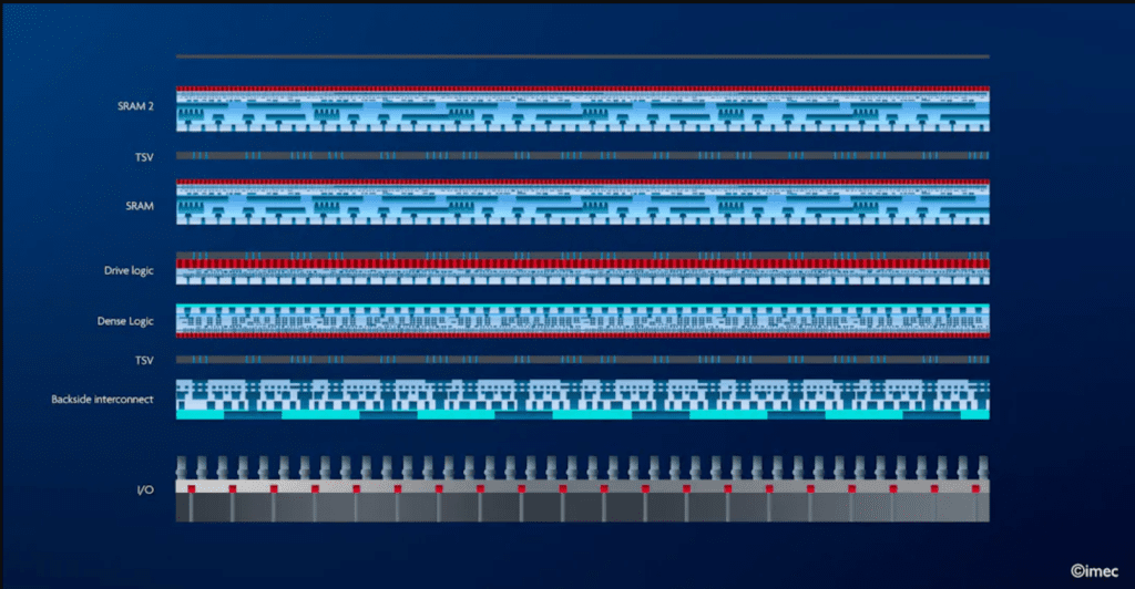
By splitting up the chip into different layers, we can optimize the process technology for each part of the chip. It allows one to bring the memory extremely close to the logic circuity. We could even consider splitting up the logic layers into two layers, one in which we optimize the transistor for density and another where we optimize for drive current. But CMOS 2.0 will require a paradigm shift on how circuits are designed, and will demand new EDA software approaching, evolving from designing circuits in a 2D horizontals plane into three dimensions.
Semiconductor Digest: Thank you.
(Cover Image: CMOS2.0 has the same ‘look and feel’ as a classical CMOS platform (Source: imec)