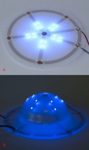
Philips is testing a technology developed by imec and CMST (imec’s associated lab at Ghent University) to create low-cost 3D LED packages. As shown at last month’s International Microelectronics Assembly and Packaging Society (IMAPS 2015) meeting, these thermoplastically deformable electronic circuits are already being integrated by Philips into LED lamp carriers, a downlight luminaire, and a omnidirectional light source.

The technology is based on meander-shaped interconnects, which are patterned using standard printed circuit board (PCB) production equipment and then sandwiched between 2D thermoplastic polymer (e.g. polycarbonate) sheets. The Figure shows one example in final form after vacuum thermoforming into a 40mm half-sphere mold.
This is a glorious example of “elegant engineering” where a clever combination of materials and processes has been integrated with highly desirable characteristics: low tooling cost, low direct material cost, easily scalable from lab to fab, low product weight, and high product resilience. This seems to represent almost a new industrial product category that combines a “package” and a PCB.
—E.K.