The IEEE IEDM conference, sponsored by the IEEE Electron Devices Society, is the world’s largest, most influential forum for the unveiling of breakthroughs in transistors and related micro/nanoelectronics devices. The theme of the 70th annual IEEE IEDM was “Shaping Tomorrow’s Semiconductor Technology.”
Advanced logic technologies
Nanosheet-based transistors, and 3D complementary FETs (CFETs) built from nanosheets, are key to continuing Moore’s Law scaling, as existing FinFET architectures are reaching their performance limits. Nanosheets are gate-all-around (GAA) transistor architectures where stacks of silicon channels are completely surrounded by the gate. They offer better electrostatic control than FinFETs, relatively high drive currents, and variable widths. CFETs, meanwhile, are highly integrated 3D designs where n-FET and p-FET nanosheets are stacked on top of one other. These stacked devices may be built monolithically (on one wafer), or sequentially (built on separate wafers and then transferred and integrated). Stacking devices essentially doubles transistor density without increasing the device footprint, which enables greater functionality and improves power efficiency and performance. At IEDM 2024, a number of papers advanced the state-of-the-art in these areas:
TSMC’s New, Industry-Leading 2nm CMOS Logic Platform: TSMC researchers unveiled the world’s most advanced logic technology. It is the company’s forthcoming 2nm CMOS (i.e., N2), platform, designed for energy-efficient computing in AI, mobile, and HPC applications. It offers a 15% speed gain (or 30% power reduction) at >1.15x chip density versus the most advanced logic technology currently in production, TSMC’s own 3nm CMOS (N3) platform, introduced in late 2022.
The new N2 platform features GAA nanosheet transistors; middle-/back-end-of-line interconnects with the densest SRAM macro ever reported (~38Mb/mm2); and a holistic, system-technology co-optimized (STCO) architecture offering great design flexibility. That architecture includes a scalable copper-based redistribution layer and a flat passivation layer (for better performance, robust CPI, and seamless 3D integration); and through-silicon vias, or TSVs (for power/signal with F2F/F2B stacking). The researchers say the N2 platform is currently in risk production and scheduled for mass production in 2H’ 25. N2P (5% speed enhanced version of N2) targets to complete qualification in 2025 and mass production in 2026.
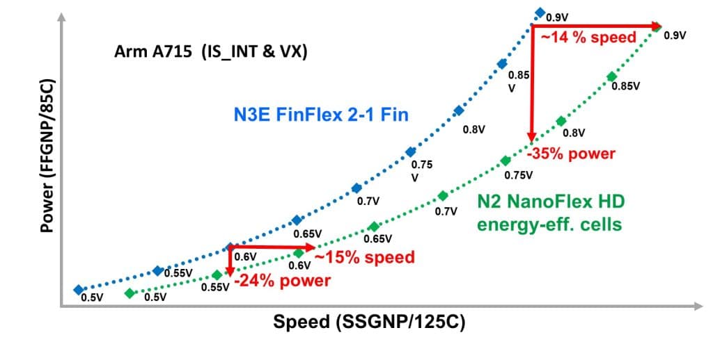
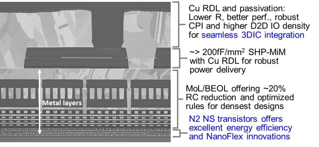
FIGURE 1a (top) is a graph showing that the new N2 high-density cells gain 14~15% speed@power vs. N3E FinFlex 2-1 fin cells across the Vdd range; a 35% power savings at higher voltage; and a 24% power savings at lower voltage. FIGURE 1b (bottom) is a cross-sectional image showing that the N2 platform’s Cu redistribution layer (RDL) and passivation provide seamless integration with 3D technologies.
(Paper #2.1, “2nm Platform Technology Featuring Energy-Efficient Nanosheet Transistors and Interconnects Co-Optimized with 3DIC for AI, HPC and Mobile SoC Applications,” G. Yeap et al, TSMC)
Extremely Scaled Transistors from Intel: Intel researchers showed that silicon can continue to support the extreme gate length scaling which future technology nodes require. They described how they built RibbonFET CMOS transistors (Intel’s version of nanosheets) with 6nm gate lengths at 45nm contacted poly pitch (CPP, the spacing between adjacent transistor gates), with no degradation of electron mobility (how fast electrons can move through a material). The researchers showed that electron mobility doesn’t degrade until 3nm Tsi (silicon thickness), below which electron scattering due to surface roughness becomes an issue. They will describe how they achieved good short channel control (≤100mV/V at <4nm Tsi), with extremely low threshold voltage at these gate lengths through clever workfunction engineering. The work shows that 3nm is a practical scaling limit for RibbonFETs.
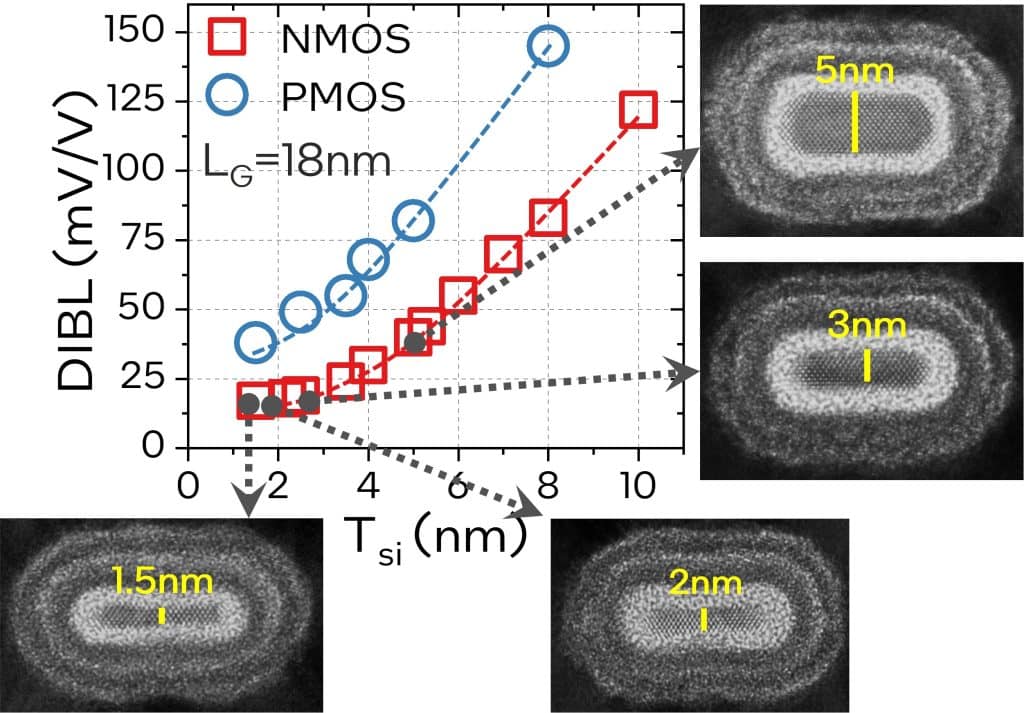
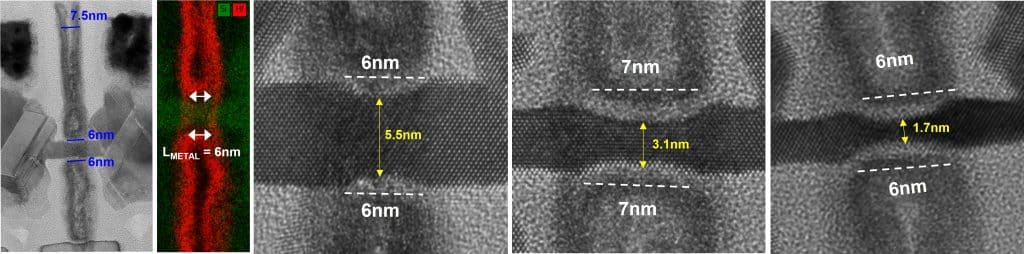
FIGURE 2a (top) illustrates the behavior of drain-induced barrier lowering (DIBL) vs. silicon thickness (Tsi) at LG=18nm. It shows a reduction as Tsi is scaled from 10nm to 1.5nm; however, DIBL reduction saturates at Tsi <4nm, below which very little gain is obtained. PMOS DIBL is elevated vs. NMOS DIBL at the same Tsi. Also shown are TEM micrographs of a 1NR transistor with various Tsi values down to 1.5nm.
The series of images shown in FIGURE 2b (bottom) are (a) TEM micrograph and EDX scan of a completed 6nm RibbonFET device on a 1NR vehicle, showing a disconnected subfin; (b – d) are high-resolution cross-section TEMs for Tsi=5.5nm, 3.1nm and 1.7nm respectively, at 6nm gate length on a 1NR vehicle.
(Paper #2.2, “Silicon RibbonFET CMOS at 6nm Gate Length,” A. Agrawal et al, Intel)
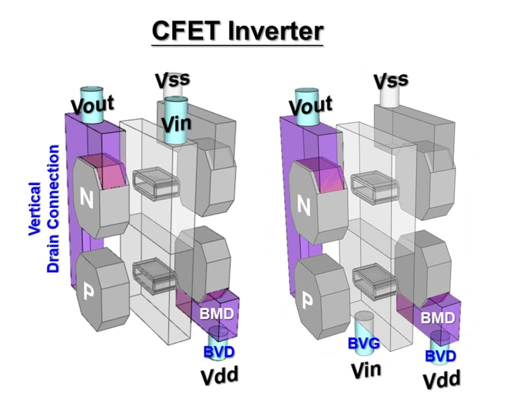
TSMC’s Fully Functional Monolithic CFET Inverter at 48nm Gate Pitch: In 2023 at the IEDM, TSMC researchers unveiled a practical, monolithic CFET architectural approach for logic technology scaling. In 2024, building on that work, they described how they built the first fully functional advanced CFET inverter at an industry-leading 48nm gate pitch. The inverter (a building block for logic circuits) is made from stacked n-FET-on-p-FET nanosheet transistors, now with backside contacts and interconnect for improved performance and increased design flexibility. The devices they built exhibited well-balanced voltage transfer characteristics up to 1.2V, and good subthreshold slope of 74-76mV/V for both n and p devices. The researchers say that this successful demonstration of fully operational CFET inverters marks an important milestone in the progress of CFET technology, paving the way for future logic technology scaling and the advancement of power, performance, area, and cost (PPAC) attributes.
FIGURE 3a shows that the inverter’s common drain is facilitated by a vertical drain-side local interconnect. PMOS power is delivered through a backside metallized drain (BMD) and backside via (BVD), while a backside gate via (BVG) offers increased flexibility for signal connections (right). These features are crucial in harnessing the full potential of power, performance, and area (PPA) benefits within the CFET architecture.
In FIGURE 3b, the center image is a TEM cross-section of the monolithic CFET interconnect architecture. The top image details the monolithic CFET contacts and local interconnects, showing a vertical metallized drain local interconnect (vMDLI); MD and VD from the frontside process, and BMD and BVD from the backside process. The bottom image focuses on the BVG implementation.
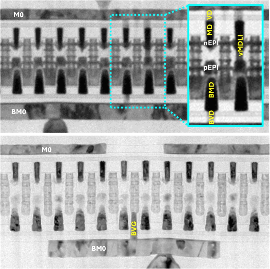
FIGURE 3c is a graph showing the voltage transfer characteristics of the monolithic CFET inverter measured up to VDD = 1.2 V.
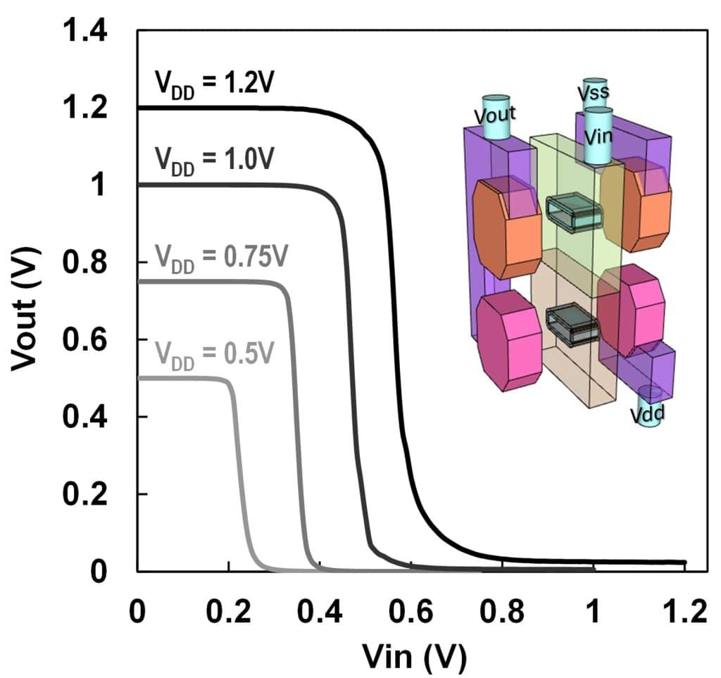
(Paper #2.5, “First Demonstration of Monolithic CFET Inverter at 48nm Gate Pitch Toward Future Logic Technology Scaling,” S. Liao et al, TSMC)
Other papers described more exploratory research into logic devices, going beyond Si-based CMOS technology:
Record Performance with Aligned Carbon Nanotube Arrays: Nanosheet scaling is currently accomplished by thinning the silicon channels, but work is ongoing to find practical ways to use already ultra-thin materials instead of Si. Recent advancements in ultra-thin channel materials such as high-density aligned carbon nanotubes (A-CNTs), 2D materials, and amorphous oxide semiconductors (AOSs), offer the potential to continue to extend Moore’s Law. A-CNT arrays have shown significant performance advantages and integration potential due to their thin body, high mobility, injection velocity and intrinsic CMOS compatibility. However, achieving high-quality gate interfaces to optimize their performance has been challenging.
A team led by Peking University used high-density A-CNT arrays to build a 100nm gate-length MOSFET with saturated on-state current (Ion) of 2.45mA/μm and peak transconductance (gm) of 3.7mS/μm, resulting in a gm/Ion ratio >1.5. This sets a new record for ultra-thin channel transistors, even surpassing the maximum gm of silicon planar FETs. The team also built a 50nm-gate-length A-CNT MOSFET with an extrinsic cut-off frequency of 302GHz, far surpassing that of silicon MOSFETs. Key to this performance was improved gate stack quality, which significantly reduced interface state density. The researchers say additional performance improvements can be obtained by further optimizing the gate stack with higher-k dielectrics having a fully passivated interface, and by using an engineered drain structure.
FIGURE 4a shows performance benchmarks of various types of emerging FETs, 4b shows the A-CNT device process flow, 4c shows the typical device structure of A-CNT FETs with LG = 100nm, and 4d is an electron microscope image of the high-density A-CNT array used in this work, with about 400 CNTs/μm and monolayer morphology.
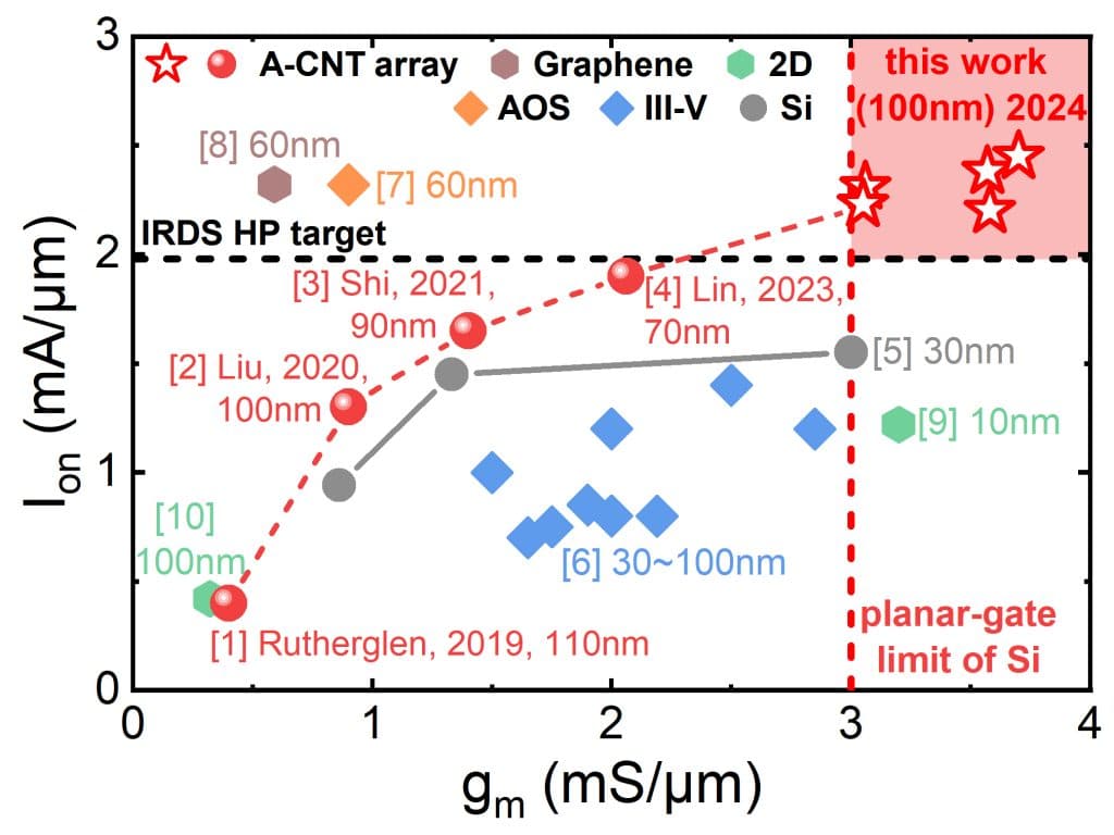
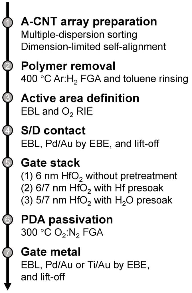
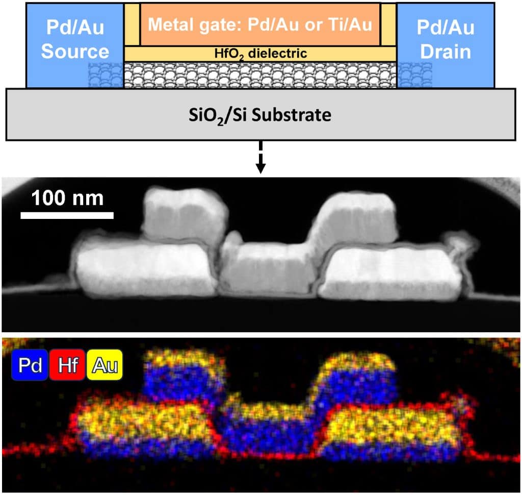

(Paper #10.1, “High-Performance Aligned Carbon Nanotube FETs with Record Transconductance of 3.7 mS/μm,” Y.F. Liu and Z. Pan et al, Peking Univ./Zhejiang Univ./Univ. of Electronic Science and Technology of China)
Record Performance with 2D Channels: Ultra-thin transition metal dichalcogenides (TMDs), such as MoS2 and WSe2, are called monolayer, or 2D, materials because they’re one just atomic layer thick. They are being extensively studied for use as the channel in extremely scaled devices because of their excellent electrical performance. However, interfacing them with other materials in a device structure is difficult because at the atomic level there are no available “dangling bonds” to use. Thus, 2D channels have been a challenge to optimize.
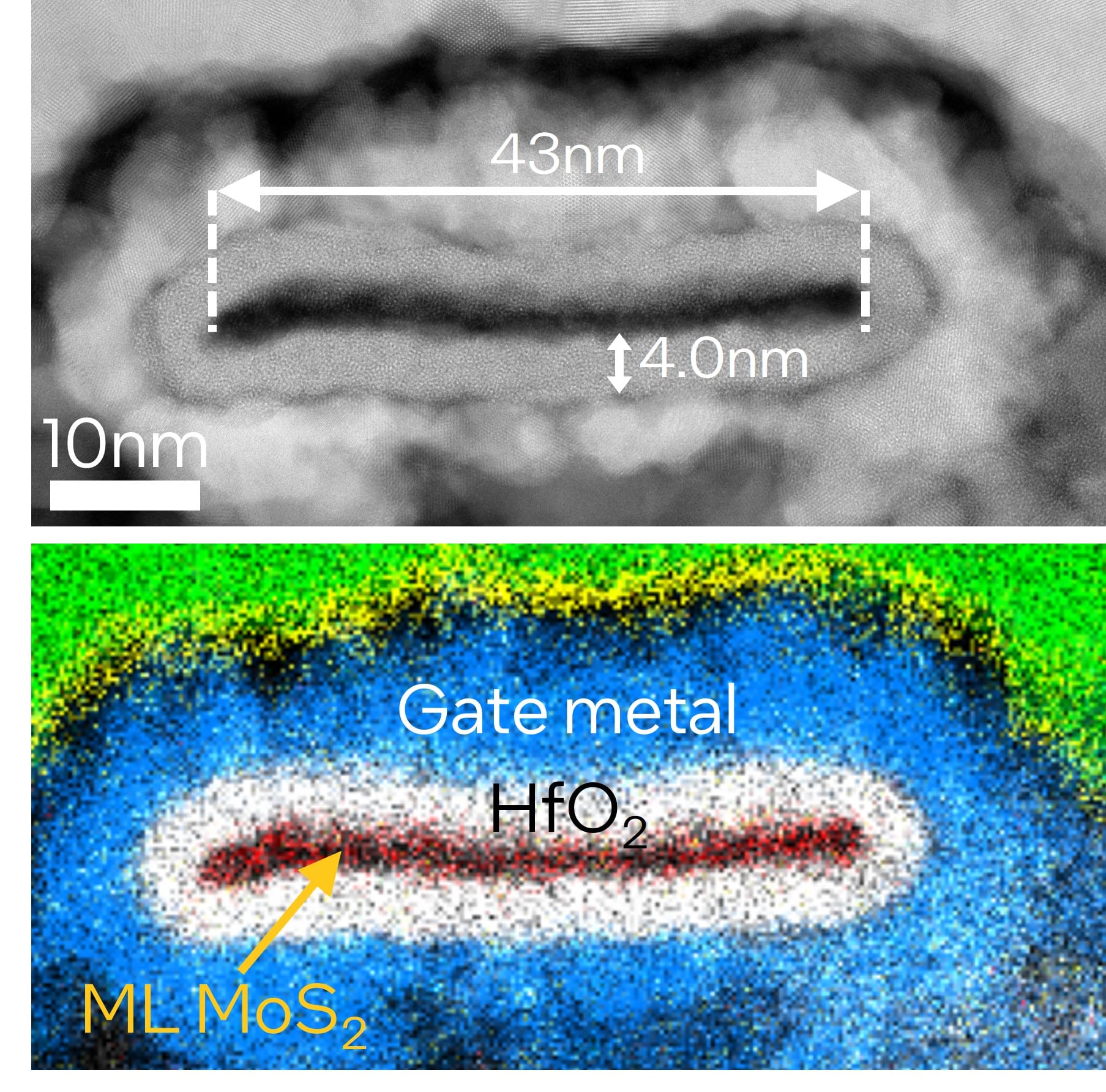
Intel researchers described how they used 1) a unique gate oxide atomic layer deposition (ALD) process and 2) a low-temperature gate cleaning process to build GAA devices that demonstrated breakthrough performance for MoS2– and WSe2-based GAA NMOS and PMOS transistors, respectively. This includes record subthreshold slope (<75mv/dec) and drain current (Idmax>900 µA/µm at <50nm gate length) in sub-1nm-thick monolayer MoS2 GAA NMOS transistors. Also, using ruthenium (Ru) source and drain (S/D) contacts, they achieved record subthreshold slope (156mV/dec) and drain current (Idmax = 132µA/µm) in a ~30nm gate-length WSe2 PMOS device. The researchers say these results both underscore the potential of 2D TMDs for use in next-generation electronics, and highlight the critical need for continued research to address the remaining scientific and technological challenges.
The images in FIGURE 5 are TEM characterizations of the record GAA NMOS device across the gate, showing a healthy, conformal GAA architecture with 43nm-wide monolayer MoS2 channel and conformal HfO2 with a thickness of ~4.0nm.

(Paper #24.3, “Gate Oxide Module Development for Scaled GAA 2D FETs Enabling SS<75mV/d and Record Idmax>900µA/µm at Lg<50nm,” W. Mortelmans et al, Intel)
Click here to read the full article in Semiconductor Digest magazine. It includes new advances in memories, computing-in-memory, high frequency and power devices, sensing and imaging and noteworthy papers on diverse topics.